Circuit Descriptions, List of Abbreviations, and IC Data Sheets
9.
9.6.3
Audio Source Selection
The signals coming out of the DEMDEC (internal demodulator/
decoder block of the Hercules) are selectable and consist of
the following (depending on the transmission):
•
DEC L/R (Can be NICAM, FM 2CS, or BTSC Stereo).
•
Mono (Refers to fallback/forced Mono in Stereo
Transmission).
•
SAP.
For L04, the assigned I/O with respect to the Hercules is as
follows:
•
SCART1 or AV1 Input assigned to Audio In 5.
•
SCART2 or AV2 Input assigned to Audio In 3.
•
Side AV Input assigned to Audio In 4.
•
External Interface Input assigned to Audio In 2.
•
SCART1 Output (EU) assigned to SCART Output.
•
SCART2 Output (EU) or Monitor Output (LA/NA/AP)
assigned to Headphone Output.
•
Constant Level Output assigned to Loudspeaker Output.
9.6.4
Video Source Selection
Video source selection is done inside the Hercules. Therefore
it provides a video switch with 3 external CVBS inputs and a
CVBS output. All CVBS inputs can be used as Y-input for Y/C
signals. However, only 2 Y/C sources can be selected because
the circuit has 2 chroma inputs.
All input signals are converted to YUV, and looped through an
external interface. This to enable picture improvement features
(like LTI/CTI) or PIP.
9.7
Video Processing
The Video Processor is basically the Hercules and the
TDA9178 (CTI/LTI). Video processing is done in these two
chips such as the Brightness Control, Contrast Control and so
on.
Some features:
•
Full YUV-loop interface (alternative functions: DVD, RGB
or Y/C).
•
Internal OSD insertion (not Saturation or Contrast
controlled).
•
Double window implementation.
•
Linear / non linear scaling for 16:9 sets.
•
Tint (hue) on UV signals (including DVD).
•
Peaking, Coring, Black \ Blue \ White-stretch.
•
Transfer-Ratio and Scavem (also on TXT).
9.7.1
Features
The features included in the Hercules are as follows:
•
Brightness Control.
•
Contrast Control.
•
Saturation Control.
•
Sharpness Control.
•
Peak White Limiter.
•
Beam Current Limiter.
•
Black Stretch (Contrast Plus).
For sets with the TDA9178, there are two extra features:
•
Luminance Transient Improvement (LTI).
•
Color Transient Improvement (CTI).
9.7.2
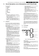
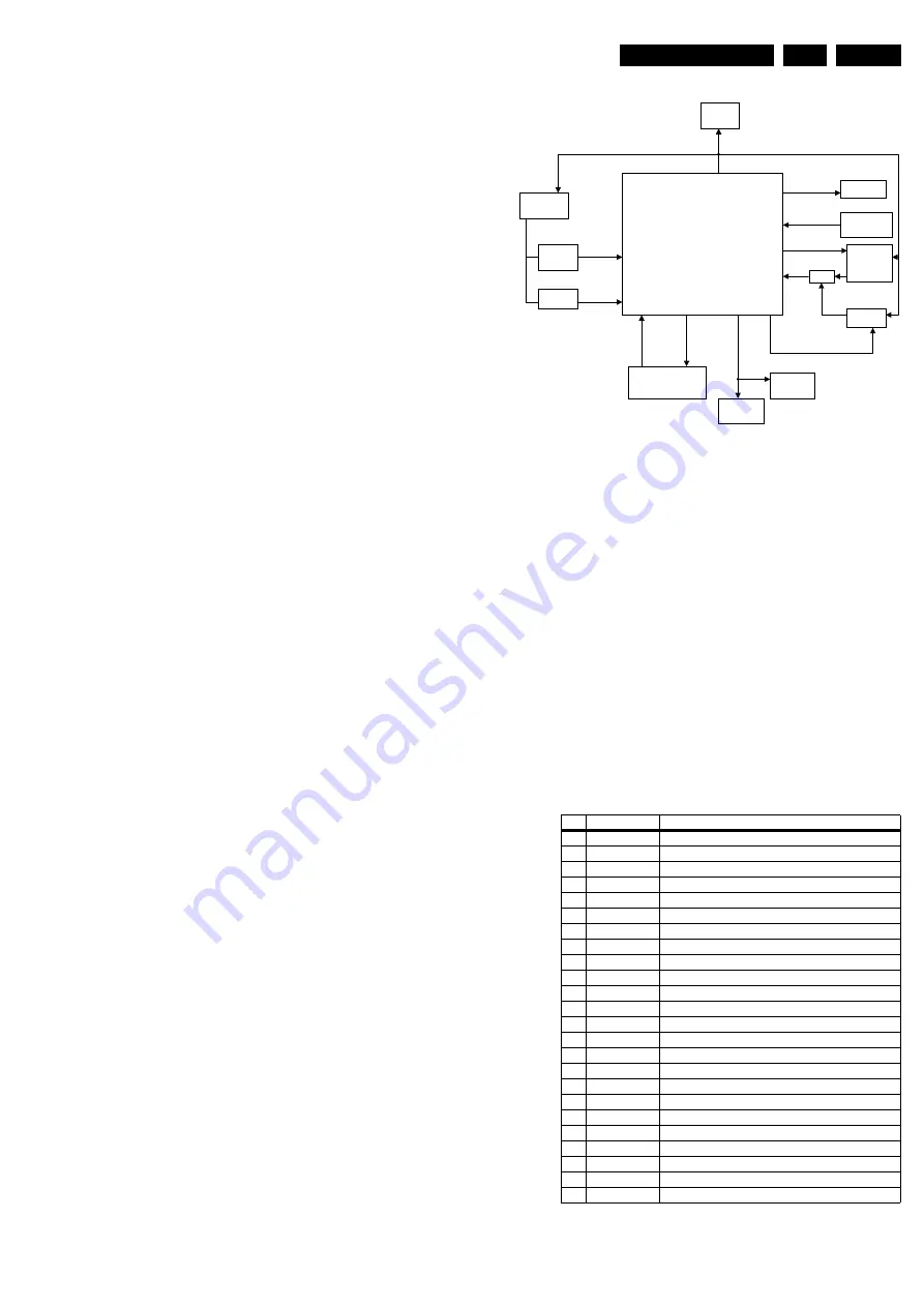
Block Diagram
Following diagram is the block diagram of the video processing
part:
Figure 9-5 Video processing block diagram
9.7.3
LTI/CTI
The TDA9178 is an I2C-bus controlled IC (INCREDIBLE chip)
with YUV interface. This IC can do mainly histogram
processing, color transient improvement (CTI) and line
transient improvement (LTI).
•
Luminance Vector Processing involves histogram function,
which provides scene dependent contrast improvement,
adaptive black and white point stretching.
•
Color Vector Processing involves skin tone correction,
green enhancement and blue stretch.
•
Spectral Processor involves step improvement processing,
contour processing, smart sharpness control, color
dependant sharpness and Color Transient Improvement.
•
Noise detector, feature mode detector and cue flash
functions.
•
Demonstration mode shows all the improvement features
in one picture.
Table 9-12 Pinning overview TDA9178
Pin
Symbol
Description
1
SC
Sandcastle input pin
2
n.c.
Not connected pin
3
ADEXT1
External AD-conversion #1 input pin
4
ADEXT2
External AD-conversion #2 input pin
5
ADEXT3
External AD-conversion #3 input pin
6
Y in
Luminance input pin
7
ADR
Address selection input pin
8
U in
-(B-Y) signal input pin
9
V in
-(R-Y) signal input pin
10
TP
Testpin, connected to ground
11
SCL
I2C-bus: clock input pin
12
n.c.
Not connected pin
13
n.c.
Not connected pin
14
SDA
I2C-bus: data input pin
15
DECDIG
Decoupling digital supply
16
V out
-(R-Y) signal output pin
17
U out
-(B-Y) signal output pin
18
V ee
Ground pin
19
Y out
Luminance output pin
20
V cc
Supply-voltage pin
21
S out
Luminance output for SCAVEM
22
CF
Cue-flash output pin
23
n.c.
Not connected pin
24
n.c.
Not connected pin
TUNER
SAW
95,94,80,79,
AUDIO
AM P
68,69
VI DEO
AUDIO
SAW
NVM
MONITOR
OUT
20 21
CRT
LTI/CTI
78,77,76,75,
74,73,72,71,70
65
86,81,
67,66
HERCULES
SW
24 25
29,30
PIP/
DVD
CVBS/AUDIO
REAR/SIDE
INPUT/OUTPUT
INPUT
RGB/CVI
42,43 44
53,54,55
57,58 59
49,50,51
E_14480_071.eps
200204
Summary of Contents for L04LAA
Page 36: ...Service Modes Error Codes and Fault Finding EN 36 L04L AA 5 E_06532_012 eps 130204 ...
Page 58: ...58 L04L AA 7 Circuit Diagrams and PWB Layouts Layout Mono Carrier Part 1 Bottom Side Part 1 ...
Page 93: ...Spare Parts List EN 93 L04L AA 10 10 Spare Parts List Not applicable ...
Page 94: ...Revision List EN 94 L04L AA 11 11 Revision List First release ...


