Circuit Descriptions, List of Abbreviations, and IC Data Sheets
9.
9.11
IC Data Sheets
This section shows the internal block diagrams and pin layouts
of ICs that are drawn as "black boxes" in the electrical diagrams
(with the exception of "memory" and "logic" ICs).
9.11.1
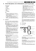
Diagram H, TDA9178 (IC7610)
Figure 9-6 Internal Block Diagram and Pin Configuration
BLOCK DIAGRAM
PIN CONFIGURATION
input-
stage
Yin
Uin
Vin
luminance
processing
Luminance vector processing
black stretch
histogram processing
gamma control
Y
saturation
correction
U,V
delay
control
smart peaking
LTI
VDC
CDS
CTI
+
spectral processing
Sout
colour
processing
output
stage
Yout
Uout
Vout
noise
measuring
featuremode
detection
supply
window
generation
calibrate
Vcc
ground
Sandcastle
I
2
C
I
2
C-control
ADext1 (low frequencies)
ADC
skin tone correction
green enhancement
blue stretch
colour vector processing
"cue flash"
ADext2 (low frequencies)
ADext3 (low frequencies)
CF
DEC
DIG
1
TDA9178
2
3
4
5
6
7
8
9
10
11
12
13
14
15
16
17
18
19
20
21
22
23
24
Sc
Nc
ADEXT1
ADEXT2
ADEXT3
Yin
ADR
Uin
Vin
TP
SCL
Nc
Nc
SDA
DEC
DIG
Vout
Uout
Vee
Yout
Vcc
Sout
CF
Nc
Nc
E_14480_075.eps
270204
Summary of Contents for L04LAA
Page 36: ...Service Modes Error Codes and Fault Finding EN 36 L04L AA 5 E_06532_012 eps 130204 ...
Page 58: ...58 L04L AA 7 Circuit Diagrams and PWB Layouts Layout Mono Carrier Part 1 Bottom Side Part 1 ...
Page 93: ...Spare Parts List EN 93 L04L AA 10 10 Spare Parts List Not applicable ...
Page 94: ...Revision List EN 94 L04L AA 11 11 Revision List First release ...

