background image

Circuit description new circuits

GB 58

L9.2A

9.

2CS : FM STEREO / FM MONO ( all standards 4.5, 5.5, 6.5 
MHz )

BTSC : MONO/STEREO/STEREO-AP

MONO/AV STEREO, BTSC DBX incorporating 2CS (two 
carrier stereo) use a TDA8841/42 BIMOS device (built-in Mono 
FM Demodulator circuit).
The Audio Module incorporates for each system a different 
multi digital sound processor.

MONO /AV STEREO: BSP3505 & TDA884x

NICAM / 2CS: MSP3415D

BTSC: TDA8841, TDA9851 and HEF4052

These IC's have an incorporate digital audio processing for 
volume, bass,  treble, balance, mute, spatial sound, incredible 
sound,  smart sound and source selection (SIF-signal, EXT1 or 
EXT2).

9.4.1

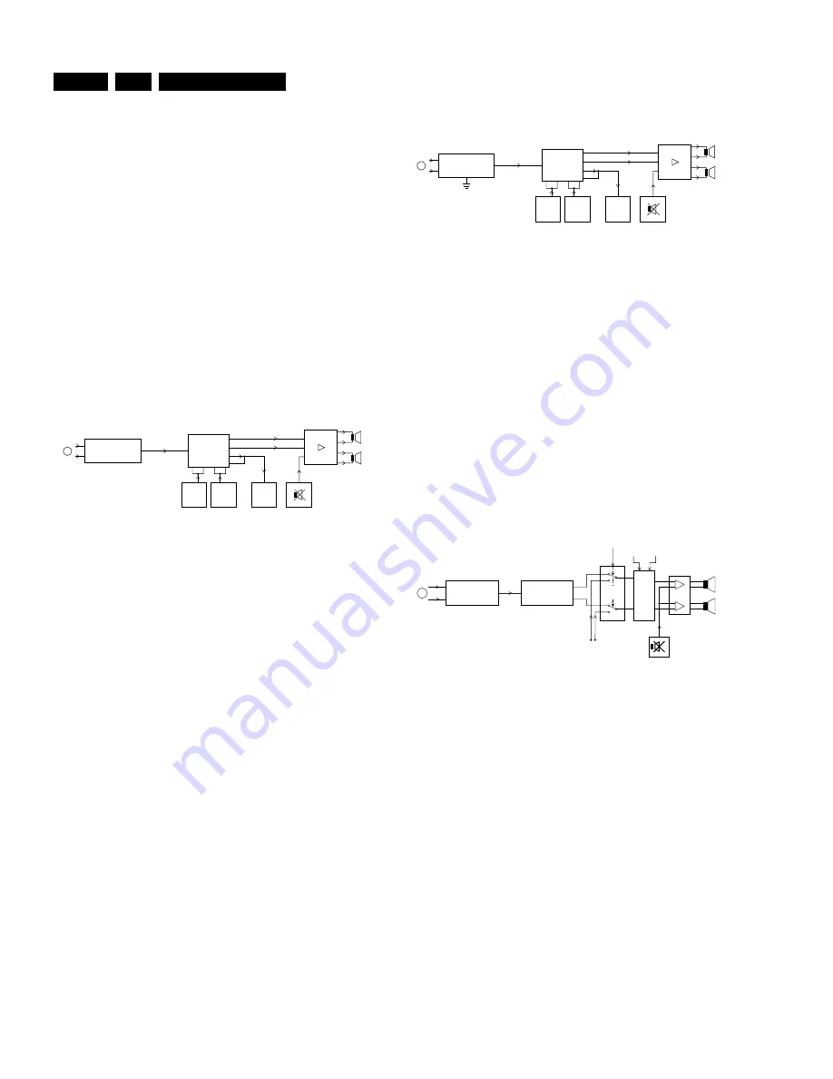
MONO / AV STEREO

This set does have the digital sound processor BSP3505, 
IC7833. 

Figure 9-10 “MONO / AV STEREO SETS”

The video IF output is present at pin 11 of the tuner 1000. This 
signal goes through a sound SAW filter and is fed to the BIMOS 
via pins 48 and 49, where the signal is demodulated. . At pin 6 
of  BIMOS IC 7250-A, the SIF signal is fed to another SAW 
filter. Signal Duall/Mono selects either SAW filter 1001 or SAW 
filter 1002.
The system hardware configuration, option code SY, is set at 
AD - Dual Mono for a Dual configuration, while option code SY 
is set at SS for the Mono configuration ( BG,I, DK, M ). Via 
Duall/Mono, a signal coming from the Micro-processor IC7600, 
is possible to switch between two Mono configurations (BG/DK 
or BG/I or DK/I). 
This signal goes back to pin 1 of the BIMOS , for further 
demodulation. The demodulated FM signal or the REAR I/O 
audio signal, ExtAudioMono at pin 2, is switched by the BIMOS 
and is present at pin 15. 
The signal at pin 15 is fed to pin 55 of IC 7833 - BSP3505 - at 
panel D1. IC 7833 performs source selection as well as audio 
processing such as volume, bas, treble, balance, tone control 
and spatial stereo. The audio output from IC 7833, pin 28 and 
pin 29, is fed to the power amplifier IC 7950 or IC7951. Pin 36 
and 37 pass the same selected signal through to the Audio-
cinches.
Signal Volume enables the output of the sound amplifier.

9.4.2

2CS

It is used on some cable television networks.
The diagram below indicates the AUDIO path for 2CS.
The CVBS + SIF signals present at pin 6 from BIMOS, -
TDA8844-, are passed through a high pass filter and are then 
fed back into pin 58 of IC 7803 (MSP3415D) for further 
demodulation. All variants of 2CS are demodulated in this IC.

Figure 9-11 “2CS”

Audio signals coming from the frontpanel are connected to pin 
49/50 of IC7803 for the Ext1Audio signals, while pin 52/53 of IC 
7861 are used for the Ext2Audio signals. IC 7803 performs 
source selection as well as audio processing such as volume, 
balance, tone control, mute, spatial stereo, incredible surround 
sound and SMART sound. The audio output from IC 7803, pin 
28 and pin 29, is fed to the power amplifier IC 7953 or IC7954. 
Pin 36 and 37 pass the same selected signal through to the 
audio-cinches.  Signal Volume enables the output of the sound 
amplifier.

9.4.3

BTSC 

The SIF signal from the BIMOS are passed through a high pass 
filter and are then fed back into pin 7 of IC 7861 (TDA9851) for 
further demodulation. This signal is present at pin 6 of BIMOS 
- TDA8841.

Figure 9-12 “BTSC”

Audio signals coming from the rear I/O panel are connected to 
pin 5/14 of IC7802 for the Ext1Audio signals. The audio output 
from IC 7802, performs the source selection via signal EXT 1 / 
2. It is possible to switch between the demodulated BTSC 
signal on the FRONT/EXT signal. Pin 3 and pin 13, are fed to 
the power amplifier IC 7954. Signal Volume enables the output 
of the sound amplifier.

9.5

Tuner and Video IF (see circuit diagram A5) 

9.5.1

Introduction:

In Figure 9.13 a simplified block diagram of the video path is 
shown. The main item in the block diagram shown in Fig.9.13 
is the video processor item 7250. The IC performs the following 
functions, video IF demodulation, chroma processing and RGB 
processing.  Additionally synchronisation processing, mono IF 
audio demodulation and audio selection takes place.
One version of video processor is used:

TDA8844 N2 for SW CENELEC BG/DK, CENELEC I 
NICAM, CENELEC BG NICAM

For a detailed block diagram of the TDA8844/8845 see Figure 
9.12.

MONO/AV STEREO

TDA 8844

R

+

L

+

R

-

L

-

16

9

13

12

7953/7954

7803

EXT. 1

AUDIO

EXT. 2

AUDIO

CL 96532047_018.eps

020699

48

49

7250-A

AUDIO OUT

15

5

3

BSP3505

52

53

49

50

58

28

29

36

37

IF

LEFT OUT

RIGHT OUT

REAR

2CS

TDA 8844

R

+

L

+

R

-

L

-

8

13

10

11

7953/7954

7803

EXT. 1

AUDIO

EXT. 2

AUDIO

CL 96532047_019.eps

020699

48

49

7250-A

(SIF)

6

5

3

MSP3415

52

53

49

50

58

28

29

36

37

IF

LEFT OUT

RIGHT OUT

15

REAR

13(R)

12(L)

CL 96532047_026.eps

250599

TDA 8841

7250-A

SIF

48

49

TDA 9851

7861

7802

7

6

SMART
SOUND

BASS

TREBLE

FRONT

EXT1 Audio L

FRONT
EXT1 Audio R

1

5

3

13

12
14

4
2

8

6

16
13

9

12

HEF

4052

7954

EXT 1/2

IF

"BTSC"

Summary of Contents for L9.2A

Page 1: ...1 Supply voltage diagram 25 Blockdiagram 26 Testpointsoverview and oscillograms 27 7 Electrical diagram s en PWB s Diagram PWB Power supply Diagram A1 28 34 37 Diversity table A1 29 Horizontal deflection Diagram A2 30 34 37 Vertical deflection Diagram A3 31 34 37 Synchronisation Diagram A4 31 34 37 Tuner en video IF TDA 8844 Diagram A5 32 34 37 Diversity table A5 33 Video processing Diagram A6 38 ...

Page 2: ...6C AI PAL 1 2 Specification of the terminal sockets 1 3 Specification of the terminal sockets 1 3 1 Inputs AV1 AV2 and Side AV Cinch CVBS yellow 1Vpp 3dB 75Ω q Cinch Audio R red 0 2 2VRMS 10kΩ q Cinch Audio L white 0 2 2VRMS 10kΩ q 1 3 2 Outputs MONITOR out Cinch CVBS yellow 1Vpp 3dB 75Ω q Cinch Audio R red 0 5VRMS 1kΩ q Cinch Audio L white 0 5VRMS 1kΩ q 1 3 3 Headphone Jack 8 600 4mW t 1 3 4 SVHS...

Page 3: ...o avoid touching the CRT hot components or heat sinks The electrical DC resistance between the mains plug and the secondary side should be checked only for sets which have a mains isolated power supply This check can be done as follows Unplug the mains cord and connect a wire between the two pins of the mains plug Set the mains switch to the on position keep the mains cord unplugged Measure the re...

Page 4: ...nt of this unit during repair is therefore not recommended 6 Be careful during measurements in the high voltage section and on the picture tube 7 Never replace modules or other components while the unit is switched on 8 When making settings use plastic rather than metal tools This will prevent any short circuits and the danger of a circuit becoming unstable 9 Wear safety goggles during replacement...

Page 5: ...Directions for use GB 5 L9 2A 3 3 Directions for use ...

Page 6: ...Directions for use GB 6 L9 2A 3 ...

Page 7: ...Directions for use GB 7 L9 2A 3 ...

Page 8: ...Directions for use GB 8 L9 2A 3 ...

Page 9: ...Directions for use GB 9 L9 2A 3 ...

Page 10: ...Directions for use GB 10 L9 2A 3 ...

Page 11: ...Directions for use GB 11 L9 2A 3 ...

Page 12: ...Directions for use GB 12 L9 2A 3 ...

Page 13: ...Directions for use GB 13 L9 2A 3 ...

Page 14: ... Test points for the frame deflection circuit A3 I1 I2 I3 etc Test points for the Tuner Video IF circuit A5 L1 L2 L3 etc Test points for the Line deflection circuit A2 P1 P2 P3 etc Test points for the power supply A1 S1 S2 S3 etc Test points for the synchronisation circuit A4 V1 V2 V3 etc Test points for the video processing circuit CRT panel A6 CRT panel B Measurements are performed under the fol...

Page 15: ...NU key again will return to the last SDM status Error buffer Pressing the OSD button on the remote control shows all OSD incl error buffer Access to SAM By pressing the CHANNEL DOWN and VOLUME DOWN buttons on the local keyboard simultaneously or pressing ALIGN on theDST DST the set switches from SDM to SAM In the SDM the following information is displayed on the screen Figure 5 3 Service Default M...

Page 16: ...ter the normal user menu TV lock installation brightness colour and contrast while SAM remains displayed in top of screen Pressing the MENU key again will return to the last SAM status Pressing the OSD button of the remote control shows only SAM in the top of screen Access to SDM Pressing the DEFAULT button on the DST SAM menu control Menu items AKB VSD Tuner White tone Geometry and Audio can be s...

Page 17: ... from left to right when an error occurs that is not yet in the error code buffer the error is written at the left side and all other errors shift one position to the right the error code buffer will be cleared in the following cases 1 exiting SDM or SAM with the Standby command on the remote control 2 transmitting the commands EXIT with the DST RC7150 3 transmitting the commands DIAGNOSE 9 9 OK w...

Page 18: ...e BIMOS 7250 D pin 40 A4 Synchronisation Timer IC 7607 or transitor 7608 is defect A7 Control 2 Note If the Collector of 7402 is shorted to the Emitter hick up noise can be heard from the power supplyIn this case the E W protection is disabled is correctly working a parabolic picture 3 Also take note of protection circuits in the line output stage If any of these circuits are activated the set wil...

Page 19: ...ys 1 Communication to the television automatic 2 Asking questions to you manually ComPair combines this information with the repair information in its database to find out how to repair the L9 2A Automatic information gathering Reading out the error buffer ComPair can automatically read out the contents of the entire error buffer Diagnosis on I2C level ComPair can access the I2C bus of the televis...

Page 20: ...red LED on the Compair interface wil light up 12 Switch on the television set with the mains switch 13 When the set is in standby Click on Start up in ComPair mode from standby in the ComPair L9 2A fault finding tree otherwise continue Figure 5 7 Figure 5 8 The set has now started up in ComPair mode Follow the instruction in the L9 2A fault finding tree to diagnose the set Note that the OSD works ...

Page 21: ...ddle of the screen till this line is just not visible The alignment of the VG2 has been completed Switch the set to Standby The values adapted at the BRIGHTNESS and the CONTRAST menu during the alignment will change back again to their default values 8 2 2 Focusing Set pattern generator e g PM5418 with Circle and Small Squares pattern and connect to aerial input with RF signal amplitude 10mv Adjus...

Page 22: ...pically this is for Secam LL The default values for these option codes are CL 4 YD 12 IF PLL OFFSET 48 8 3 5 White tone Connect a pattern generator e g PM5418 and set it to colour bar and circle pattern Set frequency for PAL 475 25MHz or 61 25MHz for BTSC with RF signal amplitude 10mv and connect to tuner aerial input Enter the SAM MENU Enter into WHITE TONE menu select item NORMAL DELTAWARM or DE...

Page 23: ...g for games possible when enabled HS Hospital Mode Possibility to block the local keyboard when enabled HT Hotel Mode Possibility to pre select the channel numbers when enabled IS Incredible Surround Incredible surround function available when enabled LV Automatic Volume Leveller AVL Menu item AVL available when enabled NI No Ident Auto Standby Set switches to standby after 10min when NI enabled N...

Page 24: ... dead During T on FET 7518 conducts Energy is stored in the primary winding 2 5 of transformer T5545 by using a linear increasing primary current The slope depends on the rectified mains voltage present across C2508 The T on period is varied to provide regulation of the drive waveform at pin 3 of IC7520 By controlling the duty cycle of the SMPS in this way the VBATT is controlled During T off FET ...

Page 25: ...eing short circuited or loaded excessively the I prim becomes too high which is detected by pin 7 As a result the primary current is limited to its maximum value and the secondary voltages will drop The voltage at pin 1 which is coupled with the output voltage will also drop When the voltage at pin 1 drops below the 9V IC7520 will stop functioning and the output voltage will rapidly drop to zero V...

Page 26: ...urther demodulation All variants of 2CS are demodulated in this IC Figure 9 11 2CS Audio signals coming from the frontpanel are connected to pin 49 50 of IC7803 for the Ext1Audio signals while pin 52 53 of IC 7861 are used for the Ext2Audio signals IC 7803 performs source selection as well as audio processing such as volume balance tone control mute spatial stereo incredible surround sound and SMA...

Page 27: ...ss see software alignment adjustments 9 5 6 PLL demodulator The IF signal is demodulated with the assistance of the PLL detector The video IF demodulator can handle both negative and positively modulated IF signals selection is achieved via the IIC bus bit MOD 9 5 7 Video buffer The video buffer is present to provide a low ohmic video output with the required signal amplitude Additionally it provi...

Page 28: ...r outputs R Y and B Y are present at pin 28 29 30 of the TV processor The auto system manager identifies PAL NTSC and SECAM colour standards and is controllable via the IIC bus Connected on pin 36 of the TV processor is the Loop Filter for the phase detector The filter chosen provides an optimal transient response which ensures both an optimum for noise bandwidth and colour acquisition time 9 6 5 ...

Page 29: ...l the signal EHT_info is used This signal is a measurement of the picture contents It is filtered by 3253 2227 As the time constant of the filter is much bigger than the frame period time the DC at the anode of 6212 represents the average value of the picture content Via 6212 and 2226 the DC voltage at pin 22 is slowly clamped For peak white limiting transistor 7263 is utilised When peak white occ...

Page 30: ... controller KeyBd1 Local keyboard control signal to micro controller KeyBd2 Local keyboard control signal to micro controller In protection mode KeyBd2 is Ground KeyBd3 Local keyboard control signal to micro controller L Power amplifier output to headphone and speaker L Power amplifier output to speaker LED LED control signal from micro controller to LED LATAM Latin America schematic PCB informati...

Page 31: ... Power Supply STANDBY Switching signal from micro controller low for standby power supply will be switched to stand by mode high for normal operation SW_OUT Selected Output signal from source SYNC Synchronisation TBD To Be Defined TREBLE Control signal for treble TXT Teletext µC Micro controller USA United States schematic PCB information only applicable for North American sets V_TUNE Tuning volta...

Page 32: ... 2407h 4822 121 70637 8 2nF 5 1600V 2408 4822 122 30103 22nF 20 63V 2409 4822 124 11575 47µF 20 160V 2410 4822 124 11767 470µF 20 25V 2411 4822 124 40255 100µF 20 63V 2412 4822 121 51385 33nF 20 100V 2413 4822 124 11845 22µF 20 250V 2414 4822 124 81145 1000µF 20 16V 2415 4822 124 81145 1000µF 20 16V 2416h 4822 126 11503 820pF 10 2KV 2416h 4822 126 12263 220pF 10 2KV 2416h 4822 126 13864 330pF 10 2...

Page 33: ... 1W 3517 4822 050 21003 10k 1 0 6W 3518 2120 106 90549 0Ω27 5 3520 4822 117 11149 82k 1 0 1W 3521 4822 116 52219 330Ω 5 0 5W 3524 4822 051 20008 jumper 0805 3525h 4822 052 10229 22Ω 5 0 33W 3528 4822 116 83868 150Ω 5 0 5W 3529 4822 050 24708 4Ω7 1 0 6W 3530 4822 116 52276 3k9 5 0 5W 3532 4822 117 11507 6k8 1 0 1W 3534 4822 117 13579 220k 1 0 1W 3536 4822 051 20273 27k 5 0 1W 3537 4822 117 10833 10...

Page 34: ...0Ω 5 0 1W 3324 4822 053 12183 18k 5 3W 3326h 4822 052 10221 220Ω 5 0 33W 3327 4822 052 11152 1k5 5 0 5W 3331 4822 051 10102 1k 2 0 25W 3332 4822 117 13577 330Ω 1 1 25W 3333 4822 051 20109 10Ω 5 0 1W 3334 4822 053 12183 18k 5 3W 3336h 4822 052 10221 220Ω 5 0 33W 3337 4822 052 11152 1k5 5 0 5W 3341 4822 052 11152 1k5 5 0 5W 3347h 4822 052 10102 1k 5 0 33W 3348 4822 052 11152 1k5 5 0 5W 3349h 4822 05...

Page 35: ...31673 HEADPHONE PLUG 0253 4822 267 31673 HEADPHONE PLUG g 2171 4822 126 13512 330pF 10 50V 2172 4822 126 13512 330pF 10 50V f 3150 4822 116 83884 47k 5 0 5W 3151 4822 050 11002 1k 1 0 4W 3152 4822 116 83884 47k 5 0 5W 3153 4822 050 11002 1k 1 0 4W ...

Reviews: