Circuit description new circuits
GB 48
L9.2E
9.
9.3.4
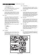
Demagnetization control (pin 8 of IC7520)
Winding 1-2 has the same polarity as the secondary winding
that supplies the load. When FET 7518 is turned off the voltage
at winding 1 becomes positive. The power supply transfers the
stored energy at the secondary side. Until the transformer is
demagnetized the voltage on the winding remains positive. At
the moment that the energy is fully transferred to the load, the
voltage at pin 9 of the transformer becomes negative.
Additionally with a certain dead time the voltage at control pin
8 of IC 7520 also drops below zero which releases the output
buffer (pin 3) and a new cycle starts.
9.3.5
Peak current limiting
An internal clamp at pin 7 allows peak current limiting to be
achieved . This pin can never exceed 1V DC and so the
maximum primary current through FET 7518, and also the
maximum output power is determined. In case of an output
being short-circuited or loaded excessively, the I-prim becomes
too high which is detected by pin 7. As a result the primary
current is limited to its maximum value and the secondary
voltages will drop. The voltage at pin 1, which is coupled with
the output voltage, will also drop. When the voltage at pin 1
drops below the 9V, IC7520 will stop functioning and the output
voltage will rapidly drop to zero.
Via start-up circuitry 3510, 3530 and 3529 the voltage
originating from the 230V AC mains is used to start-up IC7520
via the supply pin 1. As soon as this voltage reaches the 14.5V,
IC7520 starts functioning. If the load is still too much or the
output is short-circuited the same cycle will happen again. This
fault condition can be clearly identified as the power supply will
be loudly tripping.
9.3.6
Slow-start
As soon as Vpin 1 > 14.5V the SMPS will start-up. During the
slow-start procedure both the frequency and the duty cycle will
be built up slowly. The duty cycle will initially slowly increase
commencing with the absolute lowest possible duty cycle. The
maximum duty cycle is determined by C2530 at pin 11 of
IC7520, as C2530 is uncharged at start-up.
9.3.7
Standby mode
In standby mode the SMPS switches to the so-called "reduced
frequency mode" and runs at about 20 kHz. During standby the
SMPS only has to deliver a minimal level of output power. The
minimal load threshold level is determined by R3532 at pin 12.
In the L9 chassis the SMPS does not have a burst mode in
standby but only a reduced frequency mode of about 20 kHz as
stated above. In normal operation mode the internal oscillator
is around 70 kHz. This frequency is controlled by C2531 at pin
10 of IC7520 and by R3537 at pin 16 of IC7520. In standby
mode the frequency of operation is determined by R3536 at pin
15 of IC7520.
9.3.8
Protections
Over voltage protection of the secondary voltages.
After start-up the supply voltage pin 1 will be "taken over" by
winding 1-2. Pin 1 of IC 7520 is used to detect an over voltage
situation on the secondary side of the transformer. If this
voltage exceeds 17V (typical ), the output buffer is disabled,
and IC 7520 goes into over voltage protection and a complete
restart sequence is required. Check in this case IC7520, D6537
and the secondary vVBATT ( +95V ).
REMARK: In the event of the over voltage situation remaining
present, the SMPS will go in protection, start up cycle,
protection, etc. The standby led on the front of the set starts
flashing.
Under voltage protection of the secondary voltages
If the supply voltage at pin 1 of IC 7520 drops below 9V
because of a short-circuit or excessive load, the drive pulse
present at pin 3 will be disabled and IC7520 will switch off the
complete SMPS. Capacitor C2540 is charged up via start-up
resistors if3529,3510 and 3530, however once the voltage
exceeds 14.5V start up threshold, the SMPS will once again
commence a re start cycle.
In the event of the under voltage situation remaining, the SMPS
will again go in protection mode, start up cycle, protection, etc.
and so the cycle repeats. This effect is highly audible.
9.4
Audio processing
The following systems are available:
•
BASIC : FM MONO ( M,BG, I and DK : single or dual
system )
•
NICAM : FM STEREO / NICAM L/L', NICAM I, NICAM B/G,
NICAM DK
•
2CS : FM STEREO / FM MONO ( all standards 4.5, 5.5, 6.5
MHz )
BASIC models incorporating 2CS (two carrier stereo) use a
TDA8841/42 BIMOS device (built-in Mono FM Demodulator
circuit)
NICAM LL', /BG, /I versions use a TDA8845 BIMOS (AM sound
demodulator & QSS-IF circuit ; built-in)
The Audio Module incorporates the MSP3415 multi digital
sound processor. This IC incorporates digital audio processing
for volume, bass. Treble, balance, mute, spatial sound,
incredible sound, smart sound and source selection (SIF-
signal, EXT1 or EXT2).
9.4.1
Mono sets
The basic set, AM and FM, does not have the digital sound
processor MSP3415 IC7833. Instead it is equipped with a
SMART SOUND system. This circuit controls the bass and the
treble via discrete components and two control signals (BASS
and TREBLE) coming from the microprocessor.
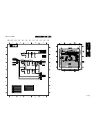
Figure 9-10 "Mono AM Sets”
The video IF output is present at pin 11 of the tuner 1000. This
signal goes through a sound SAW filter and is fed to the AM
Mono Amplifier ( Schematic A9 - IC7705 ) via pins 1 and 16,
where the signal is demodulated. Mono Audio signals,
ExtAudioMono, coming from the REAR I/O panel are fed to pin
9 of IC7705. The demodulated AM-signal or the REAR I/O
signal is switched by IC7705. One of these signals is present
at pin 6 for the I/O SCART, and present at pin 8 going to pin 2
of the BIMOS IC 7250-A. This signal is switched inside the
BIMOS to pin15.
The signal at pin 15 is fed to panel A10 - SMART SOUND +
MONO SOUND AMPLIFIER. After adjustments of the bass and
treble, the signal goes to sound amplifier 7953 ( 2W - Mono ).
AH OUT
EXT IN
SOUND
AMPLIFIER
CL 96532028_008.eps
290399
MONO AM SETS
DEMOD.
AM MONO
7705
1701
7001
7002
1000
8842
4
5
1
16
15
5
3
2
BASS
TREBLE
SMART
SOUND
LEFT
+5V
SCART
9
8
6
EXT AUDIO
MONO
1
2
µp
7280
7953
Summary of Contents for L9.2EAA
Page 5: ...Directions for use GB 5 L9 2E 3 3 Directions for use ...
Page 6: ...Directions for use GB 6 L9 2E 3 ...
Page 7: ...Directions for use GB 7 L9 2E 3 ...
Page 31: ...Schematics and PWB s GB 31 L9 2E 7 ...
Page 32: ...Schematics and PWB s GB 32 L9 2E 7 ...
Page 38: ...Schematics and PWB s GB 38 L9 2E 7 ...
Page 42: ...Schematics and PWB s GB 42 L9 2E 7 Personal notes Personal notes ...

