background image

GB

CLASS  1

LASER PRODUCT

COMPACT

DIGITAL AUDIO


Service Manual

Service

Service

Service

Service

Service

LX8200SA/

22S

TABLE OF CONTENTS

Page

Location of pc boards & Version variations ................ 1-2

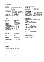
Technical Specifications ............................................. 1-3

Measurement setup .................................................... 1-4

Service Aids, Safety Instruction, etc. .......................... 1-5

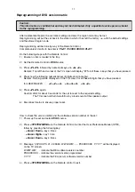
Reprogramming of DVD version matrix ..................... 1-7

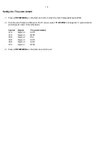
Setting the TV system default .................................... 1-8

Disassembly Instructions & Service positions .............. 2

Service Test Programs .................................................. 3

Set Block diagram ...................................................... 4-1

Set Wiring diagram ..................................................... 5-1

Key & Control Boards .................................................... 6

ECO6 Tuner Board : Systems Cenelec ..................... 7B

Supply & Main Boards ................................................... 8

Power Amplifier Board ................................................... 9

AVC Board ................................................................... 10

P-Scan Board .............................................................. 11

Set Mechanical Exploded view & parts list ................. 12

Revision List ................................................................ 13

©

 Copyright 2003 Philips Consumer Electronics B.V. Eindhoven, The Netherlands

All rights reserved.  No part of this publication may be reproduced, stored in a retrieval system or
transmitted, in any form or by any means, electronic, mechanical, photocopying, or otherwise
without the prior permission of Philips.

Published by BB 0316 Service Audio

Printed in The Netherlands

Subject to modification

AV System

3139 785 30361

Version 1.1

1. For repair information on the SD4.00SA DVD Module, refer to Service Manual

"

DVD Module SD-4.00SA_CH - 3122 785 12480

".

2. For repair information on the Subwoofer SW8000SA/00S, refer to Service

Manual "

SW8000SA/00S/01S/17S - 3139 785 30099

".

Summary of Contents for LX 8200SA

Page 1: ...ier Board 9 AVC Board 10 P Scan Board 11 Set Mechanical Exploded view parts list 12 Revision List 13 Copyright 2003 Philips Consumer Electronics B V Eindhoven The Netherlands All rights reserved No part of this publication may be reproduced stored in a retrieval system or transmitted in any form or by any means electronic mechanical photocopying or otherwise without the prior permission of Philips...

Page 2: ...8dB IF rejection 45dB Image rejection 28dB Distortion at RF 50mV M 80 5 AMPLIFIER Output power 6 ohm 1kHz 10 THD L R Center Surround 40W RMS channel Amplifier Frequency Response 3dB 250Hz 32kHz SURROUND Multichannel Stereo 3D Sound SOUND JAZZ ROCK DIGITAL CLASSIC DRAMA ACTION SCI FI CONCERT Sound effect available when playing a DVD VCD disc AUDIO INPUTS OUTPUTS Input sensitivity Aux in at 1kHz 880...

Page 3: ...gits version matrix Remark Nothing will be displayed on the TV screen for all these 8 digits that you have pressed for LX8200SA 22S 2 2 2 0 3 7 0 8 5 Press PLAY again Caution Wait for about 3 seconds for the set to reset to the required setting The TV screen will turn blue follow by a loud sound at the speaker output 6 Disconnect mains to ensure proper reset How to check the version matrix and the...

Page 4: ... the TV screen select TV SYSTEM to change the TV system default accordingly as shown in the table below Version Region TV system default 21R Region 3 AUTO 21S Region 4 NTSC 22S Region 2 PAL 30S Region 4 AUTO 33S Region 3 AUTO 37S Region 1 NTSC 3 Press SYSTEM MENU on the Remote control to exit Setting the TV system default ...

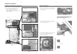
Page 5: ...tch C1 inward and slide it up in the direction as shown in Figure 3 Dismantling of the Tuner Board and Main Board and AVC Board 5 Remove 2 screws G see Figure 4 to loosen the Bracket AV PCB pos 255 4 Remove 1 screw C see Figure 2 and uncatch 2 catches C2 see Figure 4 to loosen the Main Board pos 1104 B See Service position B 6 Remove 6 screws E and 2 screws F see Figure 2 to loosen the Plate Rear ...

Page 6: ...er Tray DVD pos 105 as shown in Figure 10 3 Slide out the DVD Tray fully and remove 6 screws J see Figure 11 to loosen the DVD Module pos 1109 See Service position E 1 Remove 7 screws D to loosen the Supply Board pos 1104 A and Power Amplifier Board pos 1103 2 screws on the Plate Rear see Figure 2 5 screws on the Plate Bottom see Figure 5 6 7 8 See Service position C Figure 6 Figure 8 Figure 7 Fig...

Page 7: ... in that area This will not affect the performance of the rest of the set Dismantling of the Front Panel Assembly Figure 15 Figure 16 1 Remove 1 screw K see Figure 15 to loosen the Headphone Board pos 1105 D 2 Remove 6 screws L see Figure 15 to loosen the Volume IR Board pos 1105 C 3 Remove 2 screws M see Figure 16 to loosen the Power On Off Board pos 1105 A 4 Remove 2 screws N see Figure 16 to lo...

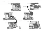
Page 8: ...vice position B Use a insulation sheet to prevent any damaged or short circuit of the boards Service position D Service position F Service position E Use a insulation sheet to prevent any damaged or short circuit of the boards DISMANTLING INSTRUCTIONS ...

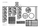
Page 9: ... value between 0 and 255 for an input signal between 0 and 5V Note If the ADC value on the NTC line is below 69 the set will go to standby mode because the temperature is too high Display shows ADC4 Value Input Line Option N SOURCE Button pressed Y Display shows ADC3 Value Input Line AmNTC CLOCK TIMER Button pressed Y Y Y N N N CLOCK TIMER Button pressed 9 Button pressed Display shows 32K Output o...

Page 10: ...hex digits Up to 16 errors can be stored in a buffer The elements can be selected by pressing the PLAY RC or RESUME RC button If the error log does not contain any fault codes LO 00000000 will be displayed Shows all error bits Selects the error bit by pressing PLAY RC or RESUME RC button Runs the Dealer Test infinitely The information returned from the module will be displayed The loop number indi...

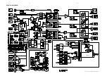
Page 11: ... MUTE_DVD DECODER MAINS TRAFO BC369 LD1117 FM 95 00 DVD DEF BC369 ADV7300 FLI2200 HIGH HEF4053BT REGISTERS INTERFACE CONTROL FORMATTER SIGNAL DIG_IN_CTRL DIG_IN_CTRL LPS COIL INPUT GENERATOR PLL CLK L R Not in all versions OUTPUT GENERATOR TMP88CU74F SUPPLY POWER AMP SYNC CORE POWER AMP 3139 119 34790_Block Diagram Sheet 130 _dd wk0240 4 1 4 1 SET BLOCK DIAGRAM ...

Page 12: ... G_Y YC1 GND YC0 FOR SET WITH LOW STANDBY HSYN VSYNC C SCL 180mm 30P 100mm BD 1MMP 2P 1 CLK_SEL DAC_RST INT_REQ side 1 24P 120mm BD 1MM FD SL GND GND GND SCART1 I2C_DATA_DVD Side FE 1002 Side FMN 1000 1 R_V R_REF 380mm 4P 140mm BD 12P 120mm AD 1 GND 180mm 1 SCART0 B_U DSD_PCM9 NC GND DSD_PCM8 NC GND DSD_LFE GND 1580 1615 1581 6P 100mm AD FOLD BD 15P DSD_Rs GND DSD_CENTRE 1 BIT_CLK DSD_CLK GND WORD...

Page 13: ...N FUNCTION C14 C0 C15 LCD PANEL INTERFACE LED BLOCK DIAGRAM LCD MODULE IC AX6120 48 15 DOTS with 38 ICONS A0 RESET VSS VDD E LED D7 D5 RW D4 D3 D2 D1 D0 1 2 3 4 5 6 7 8 9 10 11 12 13 14 15 D6 C0 C14 C15 S0 S49 6 1 KEY CONTROL BOARDS TABLE OF CONTENTS LCD Module Block diagram 6 1 LCD Module Interface Pin Function 6 1 Top Key Part Layout Circuit diagram 6 2 SACD LED Part Layout Circuit diagram 6 3 V...

Page 14: ...KEY BOARD CHIP LAYOUT A B C D E 1310 A3 1311 B3 1312 C3 1313 D3 1314 E3 1315 E2 1335 A2 1801 A1 2300 A1 2301 A1 3300 B2 3301 B2 3302 B2 3303 C2 Program Clock Timer 1 2 3 1 2 3 A B C D E A PREV NEXT STOP PLAY 3304 C2 3305 C2 3306 D2 3307 D2 3308 E2 3309 E2 From VOLUME IR 1315 1314 GND_K 3309 4K7 GND_K 3308 2K7 1310 GND_K 1311 GND_K 1313 1312 GND_K 1K8 3307 3301 220R 1 2 150R 3300 560R 3304 1335 EH ...

Page 15: ... 3139 113 3481 pt1 dd wk0227 L 1 2 3 1 2 3 A B C A B C 1580 A1 1581 B3 3530 B2 GND_D To POWER ON OFF LPS_WAKEUP 3531 C2 3532 C2 SCAD_LED 6580 B2 7580 C2 6580 1CHTDK3 1 2 3 4 5 6 7 150R 3530 5 6 LPS_LED LED_GRN D From VOLUME IR 3532 10K GND_D GND_D 7580 BC847B 10K 3531 GND_D 1581 FE ST VK N 1 2 3 4 SACD LED D 1580 FE ST VK N 3139 118 55940 8239_210_92011_01 for 3481 pt1 dd wk0227 Note Some values m...

Page 16: ... 3224 C8 D To AVC PCB Key 0 Sound 7210 A9 3216 10K GND_D 3218 1K GND_D 10K 3213 10K GND_K RC5 GND_D GND_K GND_K 7210 2212 10n GND_D 2211 10n 3222 1245 D 270R 3221 390R 220R 3220 1243 4 MT1 5 MT2 GND_D 3217 100R 3224 EVE 1244 1 3 2 560R 3223 820R 3214 GND_D D VOLUME IR 6 7 D FE ST VK N 1236 1 2 3 4 5 1 10 11 12 13 2 3 4 5 6 7 8 9 GND_K GND_K FE ST VK N 1235 2214 2n2 GND_K GND_K 1 2 GND_D GND_D 2215...

Page 17: ...OMPONENT LAYOUT HEADPHONE BOARD CHIP LAYOUT 6 6 6 6 POWER ON OFF BOARD CIRCUIT DIAGRAM POWER ON OFF BOARD COMPONENT LAYOUT POWER ON OFF BOARD CHIP LAYOUT 2 3 4 A B C A B C 1105 C2 1131 B1 3100 A2 3101 A3 3102 A4 3103 B3 3104 C3 3105 B4 3106 C4 6101 B3 LPS_LED From SACD LED LPS_WAKEUP LED_GRN LPS_Key 1 2 3 4 1 6102 B4 7100 B3 7101 B4 3100 10K 3103 22K GND_D GND_D GND_D GND_D GND_D 3101 330R BC847B ...

Page 18: ...22 051 30221 220R 5 0 062W 3221 4822 051 30271 270R 5 0 062W 3222 4822 051 30391 390R 5 0 062W 3223 4822 051 30561 560R 5 0 062W 3224 4822 117 12968 820R 5 0 62W 3300 4822 051 30151 150R 5 0 062W 3301 4822 051 30221 220R 5 0 062W 3302 4822 051 30271 270R 5 0 062W 3303 4822 051 30391 390R 5 0 062W 3304 4822 051 30561 560R 5 0 062W 3305 4822 117 12968 820R 5 0 62W 3306 4822 117 11817 1k2 1 1 16W 330...

Page 19: ...ICAL PARTS LIST KEY CONTROL BOARDS TRANSISTORS INTEGRATED CIRCUITS 7210 9322 155 82667 IR Receiver TSOP2236ZC1 7580 5322 130 60159 BC847B Note Only the parts mentioned in this list are normal service spare parts ...

Page 20: ... B V Stab B V Stab A V Stab B 10 7 MHz 10 7 MHz 35 9 Vdd Vcc1 7 23 V Stab A V Stab B 38 34 22 Vcc2 8 ECO6 Systems Cenelec 140499 V Loop FM AM RF AM Osc FM IF 1 FM IF 2 LF filter MPX buffer ampl RDS MPX 5 RDS MPX stereo clock data enable Version 3 1120 AM IF 1 AM IF 2 AM AFC 1 8 AM Frontend 2 AM FRAME AERIAL B 1103 1101 1102 A FM AM FM Discriminator 10 7 MHz Vdd FM Vcc1 Vcc Vcc2 MW LW AM RF AM Osc ...

Page 21: ...4 22n USA 22n USA C PAD 1131 T141 2106 11p 20p_LW 0R 4104 0R 41xx 2165 100n 1130 C PAD 10K 3180 2150 100n BZX284 C11 6107 T102 2127 220n 2169 2n2 100K 3170 1 I 3 O 2125 560p 5109 2 G 470R 3152 2108 100p 3125 10K 3153 470R 330R 3193 T103 120R 3167 100R 3195 7 8 33K 3176 8 5122 1 2 3 4 6 5123 1 2 3 4 6 7 5110 G 2 I 1 O 3 5115 1 2 3 4 6 7 8 2 3 4 6 7 8 5119 1 2135 100n 2163 LW 7104 BC337 40 2145 220p...

Page 22: ...ce Testprogram By selecting the TUNER TEST test frequencies will be stored as preset frequencies automatically AM FRAME AERIAL FM 75Ω FM FRONTEND Birdy Filter ECO6 Sys Cenelec layout stage 6 160501 1101 B5 1102 B5 1103 C5 1110 B4 1120 A4 1130 A5 1131 C5 1132 A4 2106 B4 2107 B3 2128 A3 2129 B3 2133 C1 2138 B1 2144 B1 2162 A4 2191 B4 3142 C2 5102 C4 5103 C4 5109 B3 5110 A2 5111 A3 5112 A2 5114 A2 51...

Page 23: ...98 021 38210 820Ω 5 0 06W 3132 4822 051 20479 47Ω 5 0 1W 3134 4822 051 20223 22kΩ 5 0 1W 3135 3198 021 31020 1kΩ 5 0 06W 3137 4822 051 20223 22kΩ 5 0 1W LW only 3141 4822 117 11148 56kΩ 1 0 1W 3142 4822 100 12159 TRIMPOT 100kΩ 3143 4822 051 20223 22kΩ 5 0 1W RDS only 3144 4822 051 10102 1kΩ 2 0 25W RDS only 3145 4822 117 11449 2 2kΩ 1 0 1W 3146 4822 051 20229 22Ω 5 0 1W 3150 4822 117 10833 10kΩ 1 ...

Page 24: ...fied supply circuitry onboard The Supply Board provides outputs 12V 5V6 5V and 3V3 supply voltages Main Board The purpose of the Main Board is to provide a means of electrical connection between the mains supply and the transformer The electronic Low Power Standby LPS circuit is also on the Main Board a Low Power Standby LPS StandbyTransformer 5905 provides the LPS supply to control the relay 1910...

Page 25: ...3 4 7215 BD438 6250 BYV28 200 24 D 4m7 2212 6205 1N4148 BC547B 7211 3233 6K8 1N4148 6206 D 3237 47K 11 12 13 14 15 16 2 3 4 5 6 7 8 9 1N4003 6240 1271 FE BT VK N 1 10 2263 1u GND_Pscan 7262 BD438 3266 12K 3216 10K GND IN OUT 3220 10K 100u 2240 7250 3K3 3203 6291 10K 3297 7212 BC547B BZX79 C5V6 3218 12K 1252 1 2 3 2254 1u 2292 22u 1K 3292 6260 3 4 5 1260 FE ST VK N 1 2 1N5392 6210 3230 3K9 3224 47K...

Page 26: ... 680R D 6291 BZX79 C5V6 D 4K7 3293 7213 BC547B 3204 D 47n 2205 D D 6216 BZX79 C15 6293 BZX79 C5V6 6290 1N4003 3230 1u 2263 1N5392 6211 T2A5 1291 BD438 7215 7252 BD438 D D 3262 390R 2295 100u EH B 1261 BD241BFP 7295 D 3231 3K9 390R 3263 Gnd_DAC 2232 1u 390R 3234 1N4003 6295 0R22 3253 Gnd_DAC 3227 1K2 BD438 7232 7261 BC547B 1N4148 6218 3212 2K2 D OUT D T4A T5A 1202 D 7260 GND IN 7210 1 2 1N5392 6212...

Page 27: ...TE 37 ONLY For 21 and 37 BLUE BLACK 1901 100u 7906 BC337 25 6904 2906 22n 6915 10n 2909 1m 470n 6908 1N4148 1910 OZ SS 112L 5901 1 2 4 3 3901 10M T2A 1905 2913 7904 BC337 40 6916 1N4003 5906 100K 3906 6902 2905 10n 2902 9901 5907 47n 9902 1N4148 6909 100n 5904 100u 2904 5903 680R 3905 BC547B BZX79 C5V6 22n 2920 7902 5 4 6 8 9 7 1 12 3907 33K BZX79 C39 6917 1 2 4M7 3903 7901 BC557B 10K 3902 2912 47...

Page 28: ... ONLY For 21 and 37 21 ONLY 3902 10K BC337 25 7906 470R 1907 B2P3 VH 1 2 3139 118 55560 8239_210_91984_01 for 3471 pt4 dd wk0333 3918 10n 2905 2909 FE ST VK N 1 2 3 4 5 5 1 4 3 6 1910 6918 5901 1 2 4 3 10M 3901 1905 T2A 1908 7904 BC337 40 1N4003 6916 5906 3910 2K2 6911 1N4148 100n 2901 6914 1N4148 6912 1N4003 1N4148 9906 6904 1N4148 100R 6906 1N4003 220n 1N4148 6910 3920 1K5 2907 100u 2908 2n2 291...

Page 29: ...0 2020 561 90365 100nF 80 20 50V 2911 4822 124 41584 100uF 20 10V 2912 4822 124 41584 100uF 20 10V 2914 4822 126 11714 4 7nF 20 2915 2020 554 90173 2 2nF 20 250V RESISTORS 3201 4822 052 10228 2R2 5 0 33W 3203 4822 116 52269 3k3 5 0 5W 3204 4822 050 21003 10k 1 0 6W 3205 4822 116 52283 4k7 5 0 5W 3209 4822 052 10108 1R 5 0 33W 3211 4822 116 52256 2k2 5 0 5W 3212 4822 116 52256 2k2 5 0 5W 3213 4822 ...

Page 30: ... BOARDS 7290 4822 130 40995 BD438 7295 4822 130 63615 BD241BFP 7901 4822 130 44568 BC557B 7902 4822 130 40959 BC547B 7904 4822 130 40855 BC337 40 7905 4822 130 44568 BC557B 7906 4822 130 40981 BC337 25 Note Only the parts mentioned in this list are normal service spare parts ...

Page 31: ...TECHNICAL REMARKS POWER AMPLIFIER BOARD TABLE OF CONTENTS Component Layout 9 2 Chip Layout 9 3 Circuit Diagram Part 1 9 4 Circuit Diagram Part 2 9 5 Electrical parts list 9 6 9 1 9 1 ...

Page 32: ...AR 2321 22u 2303 100n 3334 AP A G 2302 G 5303 1u AP G 4n7 2323 6303 1301 FE BT VK N 1 2 3 4 10n 10n 2307 2R2 3318 2R2 3320 2315 220n A 2316 220n 6305 BYV27 200 1303 B 100R 3322 100p 2389 AP BC327 25 7330 2386 100p A 100p 2387 2388 100p G VH 1300 1 2 3 50V 3331 1K 10K 3305 12K AR 2K2 3328 9306 3333 6310 GBU4DL 7002 G 3329 330R 2314 220n 5301 1u AL AP 3317 2R2 2312 47n G 3330 4K7 AL 2304 4m7 1303 A ...

Page 33: ...2 4K7 BZX79 C6V8 6338 1u 5313 G G 150K 3401 AC 2367 47n 3392 1 BC847B 7329 100u 2372 G 1303 E AS SL G 3374 1K5 220n 2355 1303 D 2359 47n 1N4148 STP16NE06 7322 C 1u 5312 4n7 2379 7302 AN7591 100p 2397 BZX79 B20 GND_SUR GND_CTR 4n7 2363 3396 6333 4 5 6 7 G G 2K2 G 1305 FE BT VK N 1 2 3 BP G 2396 100p 100p 2395 SR 2398 100p 3390 4R7 10K 3387 3K9 3406 330R 3408 3367 12K G 2360 100n 12K 3366 3388 10K 4...

Page 34: ... 4822 116 83883 470R 5 0 5W 3350 4822 051 30393 39k 5 0 062W 3351 4822 051 30393 39k 5 0 062W 3352 4822 117 12925 47k 1 0 063W 3353 4822 117 12925 47k 1 0 063W 3358 4822 117 13613 2R2 5 3359 4822 117 13613 2R2 5 3360 4822 117 13613 2R2 5 3361 4822 117 13613 2R2 5 3362 4822 116 52283 4k7 5 0 5W 3363 4822 051 30103 10k 5 0 062W 3364 4822 051 30103 10k 5 0 062W 3365 4822 051 30103 10k 5 0 062W 3366 4...

Page 35: ...ns d LINE OUT Line out with cinch socket for connection to external amplifier e CENTER OUT Center out with cinch socket for connection to active center speaker f SUBWOOFER OUTPUT Subwoofer output with cinch socket for connection to active subwoofer speaker g HEADPHONE AMPLIFIER Headphone amplifier to drive 32 ohm to 1kohm headphone The Headphone socket is not situated in this AVC Board but in the ...

Page 36: ..._A 47K 3174 3104 1K 3131 BC847BW 7150 3119 GND_A 3135 3117 8K2 100n 2102 15K 3173 7136 2166 330n GND_A 3175 10K 15K 3176 1K 3170 1K 220R TU_DATA V GND_A 2n2 3106 27K 22n 2133 2130 10K 3134 GND_A BZX79 B10 6131 3116 10K 1n 2175 I2C_CLK A_DVD BC847BW 7110 3133 10u 2108 47K 47K 5V_MUTE_1 3110 470R 3172 2158 3139 118 56960 8239_210_91846 for 3518 pt1 dd wk0315 2121 100p 1n GND_A GND_D GND_A 100p 2119 ...

Page 37: ... 3257 1K 1K 7235 BC847B 1K 3207 2231 22u 3233 1K 3209 GND_D 120p 2254 3251 12K 4K7 3244 33R 3205 4200 BC817 25 7251 BC817 25 7201 FE BT VK N 1230 1 2 3 4 NJM4556AM 7230 B 5 6 7 8 4 27K 3203 GND_A 120p 2204 1K 3210 7230 A NJM4556AM 3 2 1 8 4 2251 22u 47R 3254 47u 680K 3290 2255 100K 220R 3200 7250 BC817 25 3258 1K GND_D A_HP 1K 3256 3242 BC847BW 7237 GND_D 47K 2235 22n BC817 25 7202 D 5K6 3243 3245...

Page 38: ...19 3367 10K GND_C 7337 BC847BW GND_D 2360 100p 1K 3317 2308 33p 3312 47K 47K 3387 GND_S GND_C 3392 4K7 47K 3382 2397 47u BC847BW 7335 47u 2394 1K 3355 1K 3352 BC847B 7351 GND_S 3309 100K BC847B GND_D 68K GND_C 7301 3 4 5 6 7 3306 FE BT VK N 1332 1 2 2354 1u0 2312 100p 2307 22n 2381 4u7 3361 22n 2395 3395 1K 27K 1K 3368 22K 3314 2356 470p GND_E GND_S 1u 2345 GND_C 470u 2384 GND_C 47K 3311 GND_C 1K ...

Page 39: ...3 10K 3492 2466 DGND 3442 2K2 GND_PS 2412 100p 100n 2487 5V_P_SCAN V 12V_DVD 2461 220u V 2446 1m0 1K2 3411 2486 GND_PS 47n GND_A 3V3_DVD 5V_DVD GND_PS DGND V GND_PS 5V 220p 2437 V 5V_P_SCAN 2444 100n GND_A DGND V GND_PS DGND 5430 V GND_DAC 5VVID 100u 2440 2448 100n RT 01T 1401 1 1 4484 RT 01T 1403 1 1402 RT 01T 100n 2449 5420 4u7 V D 5445 5431 GND_A GND_A GND_PS 2492 68p LD1117DT25 7442 1 GND 3 IN...

Page 40: ...u 2564 3501 3500 GND_D 10K 3564 2568 4n7 2562 GND_D GND_D 1N4003 3 4 5 6 7 8 9 470R 3511 1530 FE BT VK N 1 10 11 12 13 14 15 2 GND_D 1N4003 6536 2K7 3571 10K 3569 470R 3520 GND_D 4500 GND_D 4530 5533 2u2 3523 470R 2531 47u D GND_D 3526 470R 470R 3502 6534 1N4148 GND_K 2532 100n 3574 10K 82p 2580 GND_D 47u 2571 GND_D 6531 1N4148 3518 470R 470R 3547 1K 3576 GND_D 5V6 5V6 10p 2573 470R 3524 GND_D 1n ...

Page 41: ...62 3689 10K 10K 3604 3647 12K 1M 3688 3V3_DAC 2675 1u 2680 100n 3692 4K7 10K 3646 10K 3698 10K 3618 3638 12K 2635 82p GND_DAC 82p 2625 AVCC_C 3674 10K 5V 1u 2667 10p 2682 10R 10K 3669 3683 3656 10K 2601 120p 2655 560p GND_OP_C 820p 2621 4602 7631 D 74LVC00AD 12 13 7 14 11 2632 82p 3635 10K DGND 2681 100n 2679 1u 2664 10p GND_OP BC847BW 7660 560p 2652 3603 12K 3664 100R 10K 3640 15K 3634 3V3_D 3V3_...

Page 42: ...C 12 8 L3 MODE 10 LOCK 16 MUTE 11 1 2 27 RESET 5 SEL STATIC 26 SPDIF 13 TEST1 4 TEST2 18 TEST3 28 25 TEST4 VDDA 22 GND_A UDA1351TS 7731 L3 CLK 9 L3 DATA A_PLL 5711 100u 330p 100n 2760 3710 75R 2762 3760 47R A_DAC 100u 5712 47u 2714 2780 1u 3713 10R D_DAC 2782 1u 2721 10u GND_A 10R 3714 100n 2709 2732 3742 10K 100p 2701 1u GND_D GND_A GND_A GND_A A_DAC A_DAC A_DAC GND_A C 2717 47u 2790 100p D_DAC 1...

Page 43: ...4822 126 13881 470pF 5 50V 2254 5322 122 33861 120pF 10 50V 2255 4822 124 40433 47uF 20 25V 2256 2020 552 94427 100pF 5 50V 2300 2238 586 59812 100nF 80 20 50V 2301 4822 126 13193 4 7nF 10 63V 2302 4822 126 14583 470nF 10 16V 2303 2020 552 94427 100pF 5 50V 2304 2020 552 96671 1uF 10 25V 2305 4822 126 13193 4 7nF 10 63V 2306 4822 126 13881 470pF 5 50V 2307 2238 916 15641 22nF 10 25V 2308 2222 867 ...

Page 44: ...uF 10 10V 2698 3198 017 34730 47nF 16V 2701 2020 552 94427 100pF 5 50V 2705 3198 016 31020 1nF 25V 2706 3198 016 31020 1nF 25V 2709 2238 586 59812 100nF 80 20 50V 2710 4822 126 14508 180pF 5 50V 2711 5322 126 11583 10nF 10 50V 2713 4822 124 41584 100uF 20 10V 2714 4822 124 40433 47uF 20 25V 2715 4822 124 41584 100uF 20 10V 2716 2238 586 59812 100nF 80 20 50V 2717 4822 124 40433 47uF 20 25V 2718 48...

Page 45: ...062W 3421 4822 051 30151 150R 5 0 062W 3422 4822 051 30151 150R 5 0 062W 3425 4822 051 30008 0R Jumper 0603 3426 4822 051 30759 75R 5 0 062W 3440 4822 051 30101 100R 5 0 062W 3442 4822 051 30222 2k2 5 0 062W 3443 4822 051 30759 75R 5 0 062W 3450 4822 051 30101 100R 5 0 062W 3451 4822 051 30222 2k2 5 0 062W 3452 4822 051 30759 75R 5 0 062W 3470 4822 051 30339 33R 5 0 062W 3471 4822 051 30479 47R 5 ...

Page 46: ...2 051 30103 10k 5 0 062W 3696 4822 051 30223 22k 5 0 062W 3697 4822 051 30103 10k 5 0 062W 3700 4822 051 30272 2k7 5 0 062W 3701 4822 117 13632 100k 1 0 62W 3710 4822 051 30759 75R 5 0 062W 3711 4822 052 10228 2R2 5 0 33W 3713 4822 051 30109 10R 5 0 062W 3714 4822 051 30109 10R 5 0 062W 3715 4822 117 12925 47k 1 0 063W 3716 4822 051 30103 10k 5 0 062W 3718 4822 051 30472 4k7 5 0 062W 3719 4822 117...

Page 47: ...57BW 7536 3139 110 53571 TMP88CU74YF LX7000S53571 7537 3198 010 42320 BC857BW 7538 3198 010 42310 BC847BW 7539 3198 010 42310 BC847BW 7610 3198 010 42310 BC847BW 7612 5322 130 44593 BC369 7613 3198 010 42310 BC847BW 7630 9322 181 11668 IC SM MC74VHC04DT 7631 9352 499 60118 IC SM 74LVC00AD 7632 9322 177 92671 IC SM CS4362 KQ 7634 4822 209 30095 IC SM LM833D 7635 4822 209 30095 IC SM LM833D 7636 482...

Page 48: ...TECHNICAL REMARKS P SCAN BOARD TABLE OF CONTENTS Top View Layout 11 2 Bottom View Layout 11 3 Circuit Diagram Part 1 11 4 Circuit Diagram Part 2 11 5 Electrical parts list 11 6 11 1 11 1 ...

Page 49: ...1 R Cr CrCb_5 38 R Cr CrCb_6 39 R Cr CrCb_7 40 R V PR_OUT_2 140 141 R V PR_OUT_3 R V PR_OUT_4 142 R V PR_OUT_5 143 144 R V PR_OUT_6 R V PR_OUT_7 145 SCLK 45 SDATA 46 SDRAM_ADDR0 103 SDRAM_ADDR1 102 SDRAM_ADDR10 91 SDRAM_ADDR2 101 SDRAM_ADDR3 100 HSYNC2_PORT1 5 HSYNC_PORT2 208 4 IN_CLK1_PORT1 IN_CLK2_PORT1 10 IN_SEL 41 OE 156 PLL_PVDD 157 PLL_PVSS 158 RESET_N 47 R Cr CrCb_0 29 32 R Cr CrCb_1 R Cr C...

Page 50: ... 7 3V3_SCAN 100p 2421 10u GND_PS 3 2 7 5 6 1 4 14 7203 A 74LVT86DB 2216 100n 3V3D_V 12 13 11 14 7 4201 3V3D_V 7200 A 74LVT74DB 100n 2413 1u 5420 1u8 150p 2420 5421 100n 2403 3402 150R 1K2 3414 100n 2218 3415 1K2 150p 2400 3416 75R 100p 2401 GND_PS 150R 3401 150R 3403 1K2 3405 3404 1K2 75R 3406 5V_P_SCAN 3V3D 3422 150R 3421 150R 150R 3423 1K2 3425 3424 1K2 4 1 5 2 75R 3426 5401 1u 7400 AD8061 3 3 4...

Page 51: ...2 2322 702 60279 RST SM 0603 RC21 27R PM5 3103 4822 117 12139 22R 5 0 062W 3104 4822 117 12139 22R 5 0 062W 3107 4822 051 30101 100R 5 0 062W 3108 4822 051 30101 100R 5 0 062W 3109 4822 117 12139 22R 5 0 062W 3110 4822 117 12139 22R 5 0 062W 3111 4822 117 12139 22R 5 0 062W 3112 4822 117 12139 22R 5 0 062W 3113 4822 117 12139 22R 5 0 062W 3114 4822 117 12139 22R 5 0 062W 3115 4822 117 12139 22R 5 ...

Reviews: