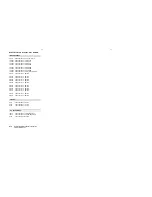
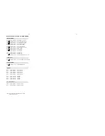
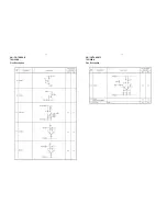
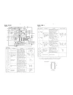
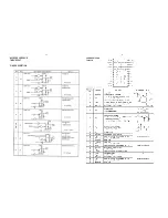
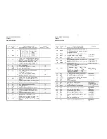
Pin No.
Pin name
Symbol
Functions
Input/Output type
1
QUAL
Demodulator quality
Type C
Good data: High, bad data : Low
Refer to output data timing
6
V
SS1
7
CMP
Comparator input
Type D
C-junction (refer to input/output circuits )
8
V
SS3
GND
2
RDATA
Demodulator data
9
T2
Test input
Type B
Open or connected to ground
10
T1
3
Vref
Reference voltage
4
MUX
Input
Type E
Type D
1/2 V
D
D1
(refer to input/output circuits)
Composite signal input (refer to input/output circuits)
11
V
D
D2
Digital power supply
4.5V to 5.5V
12
V
S
S2
13
XI
Crystal oscillator
Type A
Connects to 4.332MHz oscillator
(refer to input/output circuits)
14
XO
15
(N.C.)
Type C
16
RCLK
Demodulator clock
1187.5Hz clock (refer to the timing diagram)
5
V
DD1
Analog power supply 4.5V to 5.5V
Type A
Type B
Type D
10M
Type C
Type E
+
+
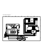
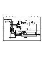
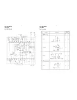
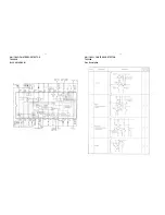
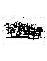
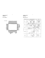
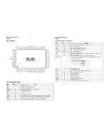
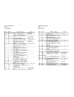
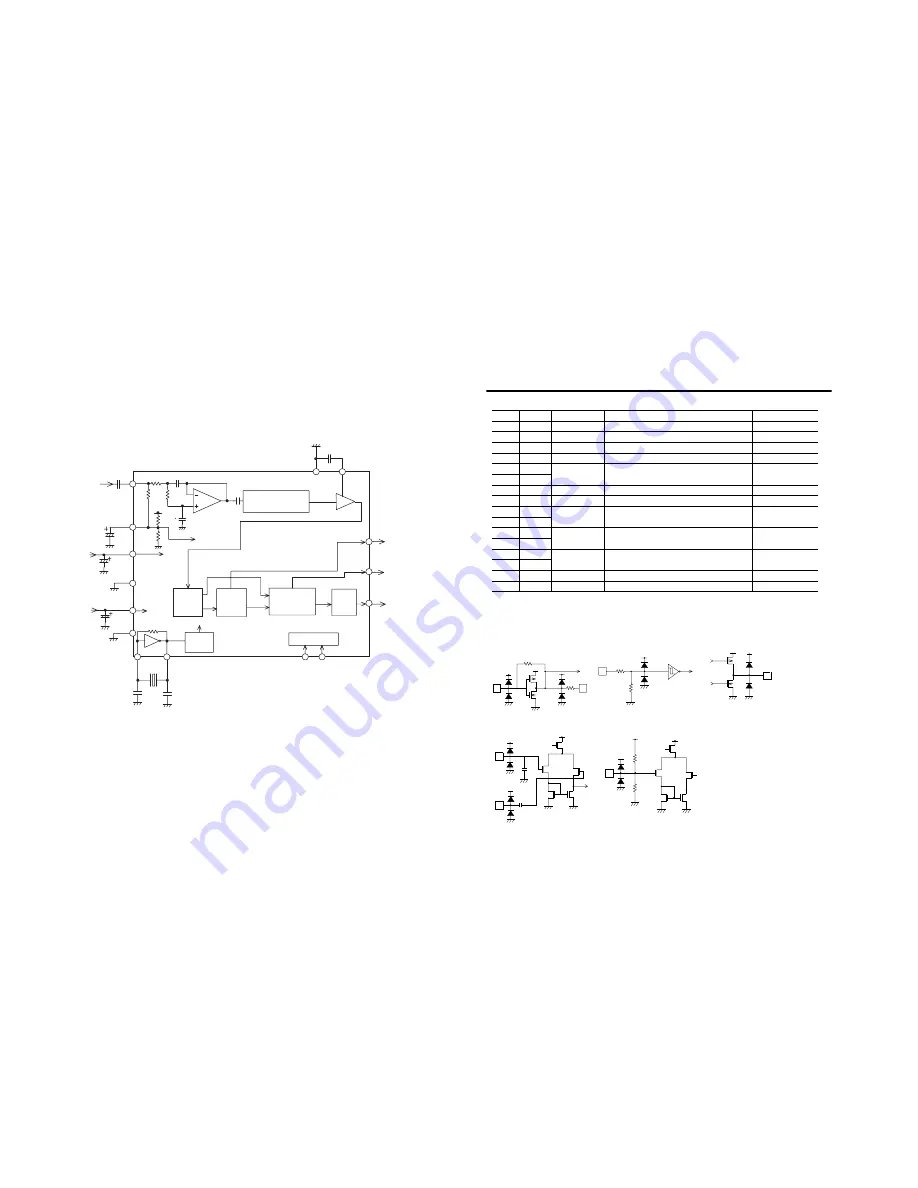
RDS/RBDS DECODER
BU1924F
RDS/RBDS DECODER
BU1924F
Pins Description
BLOCK DIAGRAM
7-8
7-8
VSS3
8th Switched
capacitor filter
Bi-phase
decoder
Measurement
circuit
Reference
clock
PLL
1187.5Hz
Differential
decoder
comparator
CMP
RCLK
QUAL
RDATA
T2
T1
560p
2.2
µ
F
120k
100k
100k
270p
V
SS
3
V
SS
2
V
SS
1
V
DD
2
V
DD
1
V
ref
MUX
Digital
Power supply
Analog
Power supply
anti-aliasing
filter
7
16
9
10
XI
XO
4.332MHz
33pF
3
3
2
1
1
33pF
13
11
12
6
3
4
5
14
1
2
8
PLL
57kHz
RDS
BU1924/F/FS
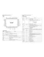
1: V
DD
1 and V
DD
2 are separated within the IC.
2: Have V
DD
2(digital power supply) of a sufficiently low impedance.
3: Match the capacitor constants with the crystal manufacturer.
Summary of Contents for MC-M350 SERIES
Page 12: ...2 2 2 2 ...
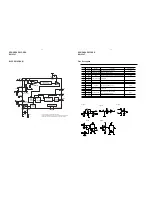
Page 14: ...4 1 4 1 SET WIRING DIAGRAM ...
Page 16: ...CIRCUIT DIAGRAM FRONT BOARD 5 2 5 2 ...
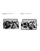
Page 17: ...LAYOUT DIAGRAM FRONT BOARD COMPONENT SIDE 5 3 5 3 LAYOUT DIAGRAM FRONT BOARD SMD SIDE ...
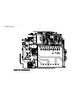
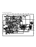
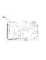
Page 20: ...6 2 6 2 CIRCUIT DIAGRAM ...
Page 21: ...6 3 6 3 POWER PCB LAYOUT ...
Page 24: ...AM FM TUNER IC TA2149BN AM FM TUNER IC TA2149BN BLOCK DIAGRAM Pins Description 7 2 7 2 ...
Page 25: ...AM FM TUNER IC TA2149BN Pins Description Pins Description AM FM TUNER IC TA2149BN 7 3 7 3 ...
Page 26: ...AM FM TUNER IC TA2149BN Pins Description AM FM TUNER IC TA2149BN Pins Description 7 4 7 4 ...
Page 31: ...DIGITAL TUNING IC TC9257F DIGITAL TUNING IC TC9257F 7 9 7 9 ...
Page 32: ...CIRCUIT DIAGRAM TUNER BOARD NON CENELEC 7 10 7 10 ...
Page 34: ...7 12 7 12 CIRCUIT DIAGRAM TUNER BOARD CENELEC ...
Page 38: ...MICROPROCESSOR TMP87EP26F MICROPROCESSOR TMP87EP26F BLOCK DIAGRAM 8 2 8 2 PINS DESCRIPTION ...
Page 39: ...8 3 8 3 MICROPROCESSOR TMP87EP26F PINS DESCRIPTION POWER DRIVER IC TA2092N ...
Page 42: ...DIGITAL SERVO PROCESSOR TC9462F BLOCK DIAGRAM 8 6 8 6 ...
Page 46: ...MICROPROCESSOR TA2153FN BLOCK DIAGRAM 8 10 8 10 ...
Page 47: ...CIRCUIT DIAGRAM MCU CD BOARD 8 11 8 11 ...
Page 48: ...LAYOUT DIAGRAM MCU CD BOARD COMPONENT SIDE 8 12 8 12 ...
Page 49: ...8 13 8 13 LAYOUT DIAGRAM MCU CD BOARD SMD SIDE ...
Page 52: ...9 2 9 2 CONNECTION PCB CIRCUIT DIAGRAM ...
Page 53: ...9 3 9 3 CONNECTION PCB LAYOUT DIAGRAM ...
Page 58: ...MAIN BOARD CIRCUIT DIAGRAM 10 4 10 4 ...
Page 59: ...10 5 10 5 TAPE PART CIRCUIT DIAGRAM ...
Page 60: ...MAIN PCB COMPONENT LAYOUT 10 6 10 6 ...
Page 61: ...MAIN PCB SMD LAYOUT 10 7 10 7 ...