

1-6
GB
WARNING
All ICs and many other semi-conductors are
susceptible to electrostatic discharges (ESD).
Careless handling during repair can reduce life
drastically.
When repairing, make sure that you are
connected with the same potential as the mass
of the set via a wrist wrap with resistance.
Keep components and tools also at this
potential.
F
ATTENTION
Tous les IC et beaucoup d’autres
semi-conducteurs sont sensibles aux
décharges statiques (ESD).
Leur longévité pourrait être considérablement
écourtée par le fait qu’aucune précaution n’est
prise à leur manipulation.
Lors de réparations, s’assurer de bien être relié
au même potentiel que la masse de l’appareil et
enfiler le bracelet serti d’une résistance de
sécurité.
Veiller à ce que les composants ainsi que les
outils que l’on utilise soient également à ce
potentiel.
ESD
D
WARNUNG
Alle ICs und viele andere Halbleiter sind
empfindlich gegenüber elektrostatischen
Entladungen (ESD).
Unsorgfältige Behandlung im Reparaturfall kan
die Lebensdauer drastisch reduzieren.
Veranlassen Sie, dass Sie im Reparaturfall über
ein Pulsarmband mit Widerstand verbunden
sind mit dem gleichen Potential wie die Masse
des Gerätes.
Bauteile und Hilfsmittel auch auf dieses gleiche
Potential halten.
NL
WAARSCHUWING
Alle IC’s en vele andere halfgeleiders zijn
gevoelig voor electrostatische ontladingen
(ESD).
Onzorgvuldig behandelen tijdens reparatie kan
de levensduur drastisch doen verminderen.
Zorg ervoor dat u tijdens reparatie via een
polsband met weerstand verbonden bent met
hetzelfde potentiaal als de massa van het
apparaat.
Houd componenten en hulpmiddelen ook op
ditzelfde potentiaal.
I
AVVERTIMENTO
Tutti IC e parecchi semi-conduttori sono
sensibili alle scariche statiche (ESD).
La loro longevità potrebbe essere fortemente
ridatta in caso di non osservazione della più
grande cauzione alla loro manipolazione.
Durante le riparazioni occorre quindi essere
collegato allo stesso potenziale che quello della
massa dell’apparecchio tramite un braccialetto
a resistenza.
Assicurarsi che i componenti e anche gli utensili
con quali si lavora siano anche a questo
potenziale.
“Pour votre sécurité, ces documents
doivent être utilisés par des spécia-
listes agréés, seuls habilités à réparer
votre appareil en panne”.
GB
Safety regulations require that the set be restored to its original
condition and that parts which are identical with those specified,
be used.
NL
Veiligheidsbepalingen vereisen, dat het apparaat bij reparatie in
zijn oorspronkelijke toestand wordt teruggebracht en dat onderdelen,
identiek aan de gespecificeerde, worden toegepast.
F
Les normes de sécurité exigent que l’appareil soit remis à l’état
d’origine et que soient utiliséés les piéces de rechange identiques
à celles spécifiées.
D
Bei jeder Reparatur sind die geltenden Sicherheitsvorschriften zu
beachten. Der Original zustand des Geräts darf nicht verändert werden;
für Reparaturen sind Original-Ersatzteile zu verwenden.
I
Le norme di sicurezza esigono che l’apparecchio venga rimesso
nelle condizioni originali e che siano utilizzati i pezzi di ricambio
identici a quelli specificati.
"After servicing and before returning set to customer perform a
leakage current measurement test from all exposed metal parts to
earth ground to assure no shock hazard exist. The leakage current
must not exceed 0.5mA."
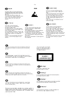
CLASS 1
LASER PRODUCT
3122 110 03420
GB
Warning !
Invisible laser radiation when open.
Avoid direct exposure to beam.
S
Varning !
Osynlig laserstrålning när apparaten är öppnad och spärren
är urkopplad. Betrakta ej strålen.
SF
Varoitus !
Avatussa laitteessa ja suojalukituksen ohitettaessa olet alttiina
näkymättömälle laserisäteilylle. Älä katso säteeseen!
DK
Advarse !
Usynlig laserstråling ved åbning når sikkerhedsafbrydere er
ude af funktion. Undgå udsaettelse for stråling.
Summary of Contents for MC-M350 SERIES
Page 12: ...2 2 2 2 ...
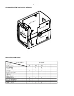
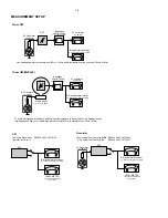
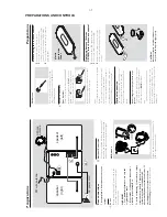
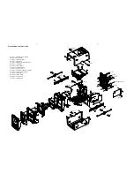
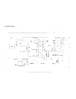
Page 14: ...4 1 4 1 SET WIRING DIAGRAM ...
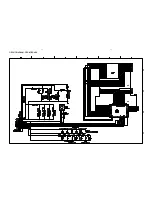
Page 16: ...CIRCUIT DIAGRAM FRONT BOARD 5 2 5 2 ...
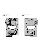
Page 17: ...LAYOUT DIAGRAM FRONT BOARD COMPONENT SIDE 5 3 5 3 LAYOUT DIAGRAM FRONT BOARD SMD SIDE ...
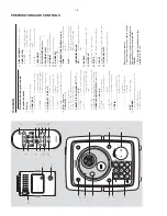
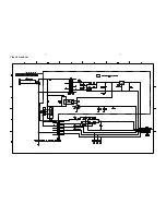
Page 20: ...6 2 6 2 CIRCUIT DIAGRAM ...
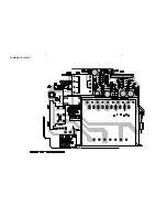
Page 21: ...6 3 6 3 POWER PCB LAYOUT ...
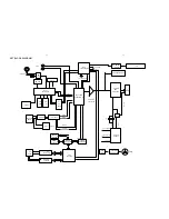
Page 24: ...AM FM TUNER IC TA2149BN AM FM TUNER IC TA2149BN BLOCK DIAGRAM Pins Description 7 2 7 2 ...
Page 25: ...AM FM TUNER IC TA2149BN Pins Description Pins Description AM FM TUNER IC TA2149BN 7 3 7 3 ...
Page 26: ...AM FM TUNER IC TA2149BN Pins Description AM FM TUNER IC TA2149BN Pins Description 7 4 7 4 ...
Page 31: ...DIGITAL TUNING IC TC9257F DIGITAL TUNING IC TC9257F 7 9 7 9 ...
Page 32: ...CIRCUIT DIAGRAM TUNER BOARD NON CENELEC 7 10 7 10 ...
Page 34: ...7 12 7 12 CIRCUIT DIAGRAM TUNER BOARD CENELEC ...
Page 38: ...MICROPROCESSOR TMP87EP26F MICROPROCESSOR TMP87EP26F BLOCK DIAGRAM 8 2 8 2 PINS DESCRIPTION ...
Page 39: ...8 3 8 3 MICROPROCESSOR TMP87EP26F PINS DESCRIPTION POWER DRIVER IC TA2092N ...
Page 42: ...DIGITAL SERVO PROCESSOR TC9462F BLOCK DIAGRAM 8 6 8 6 ...
Page 46: ...MICROPROCESSOR TA2153FN BLOCK DIAGRAM 8 10 8 10 ...
Page 47: ...CIRCUIT DIAGRAM MCU CD BOARD 8 11 8 11 ...
Page 48: ...LAYOUT DIAGRAM MCU CD BOARD COMPONENT SIDE 8 12 8 12 ...
Page 49: ...8 13 8 13 LAYOUT DIAGRAM MCU CD BOARD SMD SIDE ...
Page 52: ...9 2 9 2 CONNECTION PCB CIRCUIT DIAGRAM ...
Page 53: ...9 3 9 3 CONNECTION PCB LAYOUT DIAGRAM ...
Page 58: ...MAIN BOARD CIRCUIT DIAGRAM 10 4 10 4 ...
Page 59: ...10 5 10 5 TAPE PART CIRCUIT DIAGRAM ...
Page 60: ...MAIN PCB COMPONENT LAYOUT 10 6 10 6 ...
Page 61: ...MAIN PCB SMD LAYOUT 10 7 10 7 ...