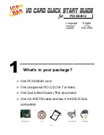
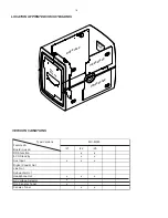
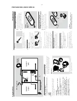

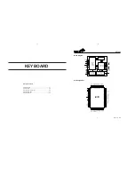
PREPARATIONS AND CONTROLS
1-7
Pr
eparations
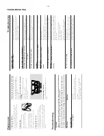
speaker
(right
)
speaker
(left)
AC power cord
AM loop
antenna
FM wire antenna
A
B
C
Rear connections
The type plate is located at the rear of the
system.
A
Po
w
e
r
Bef
ore connecting the
AC
po
w
er cord to the
wall outlet, ensure that all other connections
ha
ve
been made
.
WARNING!
–F
or optimal performance
, use only the
original po
wer cable
.
–N
ev
er mak
e
or change an
y connections
with the po
wer s
w
itched on.
To
av
oid o
verheating of the system
, a safety
circuit has been built in.
Therefor
e
, your
system may s
w
itch to Standb
y mode
automatically under e
xtreme conditions
.
If
this happens
, let the system cool do
wn
befor
e r
eusing it
(not av
ailable for all ver
sions)
.
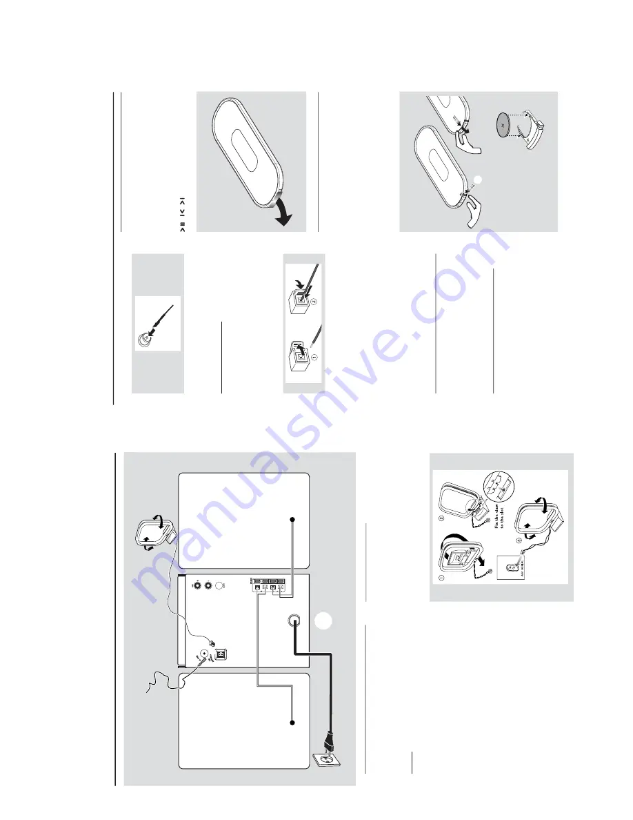
B
Antennas Connection
Connect the supplied
AM loop antenna and FM
antenna to the respecti
ve
ter
minals.
Adjust the
position of the antenna f
or optimal reception.
AM Antenna
Position the antenna as far as possible from a
TV
,
VCR or other r
adiation source
.
Pr
eparations
FM Antenna
For better FM stereo reception, connect an
outdoor FM antenna to the FM
AERIAL (FM
ANTENNA) ter
minal.
C
Speak
ers Connection
Fr
ont Speak
ers
Connect the speak
er wires to the SPEAKERS
ter
minals,
r
ight speak
er to "
RIGHT
" and left
speaker to
"
LEFT
", colored (mar
ked) wire to
"
+
" and b
lack (unmar
ked) wire to "
-
".
Fully inser
t the str
ipped por
tion of the speak
er
wire into the ter
minal as sho
wn.
Notes:
–
For optimal sound perf
or
mance
, use the supplied
speaker
s.
–
Do not connect more than one speak
er to any
one pair of
+
/
-
speak
er ter
minals
.
–
Do not connect speak
er
s with an impedance
lower than the speak
er
s supplied.
Please ref
er to
the SPECIFIC
ATIONS section of this manual.
Optional connection
The optional equipment and connecting cords
are not supplied.
Ref
er to the oper
ating
instr
uctions of the connected equipment
fo
r
details.
Connecting other equipment to y
our
system
Connect the audio left and
ri
ght OUT ter
minals
of a
TV
, VCR,
Laser Disc pla
yer
, D
V
D pla
yer or
CD Recorder to the
A
UX
ter
minals.
Note:
–
If you are connecting equipment with a mono
output (a single audio out ter
minal),
connect it to
the
A
U
X left ter
minal.
Alter
natively
, you can use a
“single to double
” cinch cab
le (the output sound still
remain mono).
Bef
or
e using the r
emote contr
ol
1
Pull out the plastic protecti
ve
sheet.
2
Select the source y
ou wish to control
by
pressing one of the source select k
eys on the
remote control (f
or example CD
, TUNER).
3
Then select the desired function (f
or example
,
,
).
Replacing batter
y (lithium
CR2025) into the r
emote contr
o
l
1
Pull out the knob
A
slightly to the left.
2
Pull out the batter
y compar
tment
B
.
3
Replace a new batter
y and full
y inser
t the
batter
y compar
tment back to the or
iginal
position.
plastic
pr
otectiv
e
sheet
CA
UTION!
Batteries contain chemical substances
, s
o
the
y should be disposed off pr
operly
.
A
CR
20
25
LIT
H
IU
M
B
Summary of Contents for MC-M350 SERIES
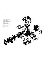
Page 12: ...2 2 2 2 ...
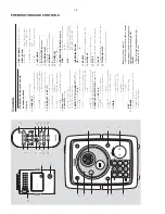
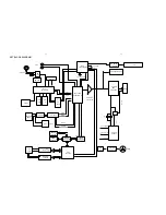
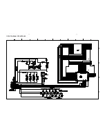
Page 14: ...4 1 4 1 SET WIRING DIAGRAM ...
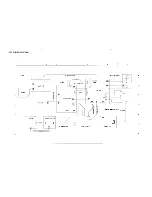
Page 16: ...CIRCUIT DIAGRAM FRONT BOARD 5 2 5 2 ...
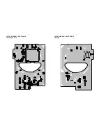
Page 17: ...LAYOUT DIAGRAM FRONT BOARD COMPONENT SIDE 5 3 5 3 LAYOUT DIAGRAM FRONT BOARD SMD SIDE ...
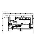
Page 20: ...6 2 6 2 CIRCUIT DIAGRAM ...
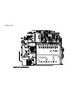
Page 21: ...6 3 6 3 POWER PCB LAYOUT ...
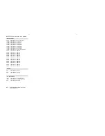
Page 24: ...AM FM TUNER IC TA2149BN AM FM TUNER IC TA2149BN BLOCK DIAGRAM Pins Description 7 2 7 2 ...
Page 25: ...AM FM TUNER IC TA2149BN Pins Description Pins Description AM FM TUNER IC TA2149BN 7 3 7 3 ...
Page 26: ...AM FM TUNER IC TA2149BN Pins Description AM FM TUNER IC TA2149BN Pins Description 7 4 7 4 ...
Page 31: ...DIGITAL TUNING IC TC9257F DIGITAL TUNING IC TC9257F 7 9 7 9 ...
Page 32: ...CIRCUIT DIAGRAM TUNER BOARD NON CENELEC 7 10 7 10 ...
Page 34: ...7 12 7 12 CIRCUIT DIAGRAM TUNER BOARD CENELEC ...
Page 38: ...MICROPROCESSOR TMP87EP26F MICROPROCESSOR TMP87EP26F BLOCK DIAGRAM 8 2 8 2 PINS DESCRIPTION ...
Page 39: ...8 3 8 3 MICROPROCESSOR TMP87EP26F PINS DESCRIPTION POWER DRIVER IC TA2092N ...
Page 42: ...DIGITAL SERVO PROCESSOR TC9462F BLOCK DIAGRAM 8 6 8 6 ...
Page 46: ...MICROPROCESSOR TA2153FN BLOCK DIAGRAM 8 10 8 10 ...
Page 47: ...CIRCUIT DIAGRAM MCU CD BOARD 8 11 8 11 ...
Page 48: ...LAYOUT DIAGRAM MCU CD BOARD COMPONENT SIDE 8 12 8 12 ...
Page 49: ...8 13 8 13 LAYOUT DIAGRAM MCU CD BOARD SMD SIDE ...
Page 52: ...9 2 9 2 CONNECTION PCB CIRCUIT DIAGRAM ...
Page 53: ...9 3 9 3 CONNECTION PCB LAYOUT DIAGRAM ...
Page 58: ...MAIN BOARD CIRCUIT DIAGRAM 10 4 10 4 ...
Page 59: ...10 5 10 5 TAPE PART CIRCUIT DIAGRAM ...
Page 60: ...MAIN PCB COMPONENT LAYOUT 10 6 10 6 ...
Page 61: ...MAIN PCB SMD LAYOUT 10 7 10 7 ...