background image

AMP Board -- Layout Diagram

12-3

12-3

Summary of Contents for MCD1065/51/98

Page 1: ...ant Safety Precautions 3 1 to 3 2 4 Safety Check After Servicing 4 1 6 Standard Notes For Servicing Lead Free Requirements Handling Flat Pack IC 6 1 to 6 4 5 Safety Information General Notes Lead Free 7 Direction of Use 7 1 to 7 2 8 Cabinet Disassembly Instructions 8 1 to 8 2 12 AMP Board 9 Troubleshooting 9 1 to 9 2 10 Block Diagram 10 1 11 Wiring Diagram 11 1 13 Display Board 14 Power Board Layo...

Page 2: ...r Repair Used 51 51 58 58 61 61 79 79 93 93 94 94 96 96 98 98 37 37 12 10 C C M M C C M M 12 10 05 05 Feature diffrence RDS AMP Board Decoder Board Power Board DTS VOLTAGE SELECTOR ECO STANDBY DARK Type Versions MCD1065 Technical Specification and Connection Facilities 1 1 Display Board Decoder Board DVD Loader Display Board AMP Board Power Board ...

Page 3: ...ut power 10 THD table 2 Set Type Number Stroke Versions Power ROP Power Volume Max Remark MCD1065 All version 2x5W 2x12W 2 1 2 Styling Forms and Functions MCD20100 DCD2030 appearances are defined in their respective MUS MUS is the leading document where product appearance is applicable Features Products MCD1065 Stroke versions l l A Design Refer to MUS 3 for details Front y a r T g n i d a o L e v...

Page 4: ...al Displa y and LED Indications tbc Control keys on the set are 1 Standby On 2 Eject 3 Play Pause 4 Next 5 Pre 6 FF 7 FB 8 Source Disc USB Dock FM Aux MP3 9 Stop 10 Volume Knob There is local display LCD reuse DCD322 LCD 2 1 5 ACCESSORIES tbc Model MCD1065 Stroke Version All Version n o i g e R Power Cord 1 8M Audio cable 3 5mm audio 0 5M AV cable Video out only 1 5M Remote Control 40keys Battery ...

Page 5: ...7th Edition For 61 Korea K 60065 6th Edition For 96 Taiwan CNS 14408 IEC 60065 7th Edition 2 4 EMC Requirements Where applicable For 12 EU 05 UK 51 Russia EN55013 2001 EN55020 2002 For 37 US Canada FCC15 For 55 LATAM 78 Brazil CISPR13 For 98 AP 69 Singapore 75 Australia CISPR13 For 61 Korea CISPR13 20 For 93 China GB 13837 CISPR13 For 96 Taiwan CNS 13439 CISPR13 2 5 ESD Requirements The product sh...

Page 6: ...by or ON OFF button of the set 4 Failures that disappear only by unplugging the AC mains cord and or power sources are not acceptable 2 6 Environmental Condition The environmental condition requirements and test method is according to UAN D1590 Ambient temperature max 40 C all climates Apparatus acc to spec 5 to 35 C Vibration test acc IEC 60 068 2 6 operational vibration test to be proceeded in o...

Page 7: ...dia 2 100 310Vac limit India compatible with up cost used only for India Frequency 47 63Hz EU 12 round 2 pin All requirements per defined for each country should be met with sufficient testing 3 1 2 Surge Immunity Lightning Test The product shall withstand mains interference s of Differential mode 2kV 2 ohm criteria C for Europe 6kV 12 ohm criteria C for NAFTA Parameters Bi wave Open circuit volta...

Page 8: ...ance criterion B Variation 0 100 dip at T event 5 Sec Performance criterion C Additional for USA apparatus See 3135 019 8029 Reliability evaluation Variation 0 100 dip at T event 100 mSec in standby mode Performance criterion B Requirement No misoperation and no interference of user in order to guarantee continuation of performed function Reference IEC61000 4 11 For measuring method refer to UAN D...

Page 9: ...ine Out Left Right 1000mV 200mV CD MP3 3dB track Audio Disc 1 Track 1 Headphone 15mW 2 dB RL 32Ω S H 0 2 e v a w e n i s z H K 1 B d 3 B S U AUX1 back 1V Rin 22kΩ MP3_link front 500mV 1000mV Rin 22kΩ IPOD Docking 750mV Rin 22kΩ Output Power 1 At THD 10 1kHz sinewave MCD1065 ROP MCD1065 Max Power 30 2 Main Operation for all version rms 5W 1dB 2x12W 1dB At Cold Condition with 10 THD Tuner output pow...

Page 10: ... luminance delay 2T pulse 20ns 20ns Subcarrier locked unlocked 75 Color bar locked locked k c a l B 0 l e v e L C D 1V 1V 3 2 2 2 Component Video Y Pb Pr Description Test Signal Specification Interlace Progressive NTSC PAL 0 1 V m 0 0 0 1 0 1 V m 0 0 0 1 e t i h W 0 0 1 t u p t u o e d u t i l p m A 0 1 V m 0 0 7 0 1 V m 4 1 7 e t i h W 0 0 1 r a b e t i h W PbPr peak to peak 75 Color bar 525mV 10...

Page 11: ... i l p m A 3 2 z H k 5 7 v e D q r F V m 1 F R n o i t r o t s i D Overall Frequency Response 63Hz 12 5KHz 3 dB Channel separation 400 1000 5000 Hz RF input 68 dBf 26 30 20 20 26 18 dB Frequency MHz Noise Limited Sensitivity 26 dB Image Rejection IF Rejection Large Signal Handling Selectivity S9 300 kHz 2 2 f B d 6 1 1 4 6 0 3 8 1 m o N M F 1 8 1 f B d 8 0 1 5 4 5 2 2 2 m i L 0 8 8 2 2 f B d 6 1 1...

Page 12: ...the pickup lens when the diode is turned on Do not look directly at the laser beam CAUTION Use of controls and adjustments or doing procedures other than those specified herein may result in hazardous radiation exposure Location Inside Top of Blu Ray mechanism Do not look directly at the laser beam coming from the pickup or allow it to strike against your skin Drive Mechanism Assembly Laser Beam R...

Page 13: ... Important Important Safety Precautions Read and understand all instructions before you use your home theater If damage is caused by failure to follow instructions the warranty does not apply Safety Riskof electricshock or fire Never expose the product and accessories to rain or water Never place liquid containers such as vases near the product If liquids are spilt on or into the product disconnec...

Page 14: ...ic products Please act according to your local rules and do not dispose of your old products with your normal household waste Correct disposal of your old product helps to prevent potential negative consequences for the environment and human health Your product contains batteries covered by the European Directive 2006 66 EC which cannot be disposed with normal household waste Please inform yoursel...

Page 15: ... and externally exposed accessible parts RF terminals antenna terminals video and audio input and output terminals microphone jacks earphone jacks etc is lower than or equal to the specified value in the table below Measuring Method Power ON Insert load Z between B earth ground power cord plug prongs and exposed accessible parts Use an AC voltmeter to measure across the terminals of load Z See Fig...

Page 16: ...e sure that during repair you are at the same potential as the mass of the set by a wristband with resistance Keep components and tools at this same potential Available ESD protection equipment Complete kit ESD3 small tablemat wristband 4822 310 10671 Wristband tester 4822 344 13999 Be careful during measurements in the live voltage section The primary side of the power supply including the heatsi...

Page 17: ...older paste is required please contact the manufacturer of your solder equipment In general use of solder paste within workshops should be avoided because paste is not easy to store and to handle Use only adequate solder tools applicable for lead free solder alloy The solder tool must be able To reach at least a solder temperature of 400 C To stabilize the adjusted temperature at the solder tip To...

Page 18: ... this and more technical information within the magazine chapter workshop news For additional questions please contact your local repair helpdesk How to Remove Install Flat Pack IC 1 Removal With Hot Air Flat Pack IC Desoldering Machine 1 Prepare the hot air flat pack IC desoldering machine then apply hot air to the Flat Pack IC about 5 to 6 seconds Fig S 1 1 2 Remove the flat pack IC with tweezer...

Page 19: ...e flat pack IC you can remove it easily Fig S 1 3 2 Affix the wire to a workbench or solid mounting point as shown in Fig S 1 5 3 While heating the pins using a fine tip soldering iron or hot air blower pull up the wire as the solder melts so as to lift the IC leads from the CBA contact pads as shown in Fig S 1 5 4 Bottom of the flat pack IC is fixed with glue to the CBA when removing entire flat ...

Page 20: ...lectrostatic charge during unpacking or repair work 1 Ground for Human Body Be sure to wear a grounding band 1 M that is properly grounded to remove any static electricity that may be charged on the body 2 Ground for Workbench Be sure to place a conductive sheet or copper plate with proper grounding 1 M on the workbench or other surface where the semi conductors are to be placed Because the static...

Page 21: ...k Tune to a radio station h Start or pause play i VOL Adjust volume Adjust time j DBB Turn the dynamic bass enhancement on or off Select a preset sound effect k SOURCE Select a source Disc USB tuner or MP3 link l Open or close the disc compartment Overview of remote control a Switch the micro system on off Switch to standby mode or Eco Power standby b DISC DISC MENU FM USB MP3 LINK Select the sour...

Page 22: ...e supplied speakers only Connect only speakers with impedance that is the same or higher than the supplied speakers Refer to the Specifications section of this manual Insert the speaker wires completely into the speaker input sockets on the back of the unit Connect TV Connect through composite video Connect the supplied composite video cable to the VIDEO OUTsocket on this unit the video input sock...

Page 23: ...ed unhooked unlocked released unplugged unclamped or desoldered Axx Screw CNxx Jxx CONxx Connector D3 5X12BA is specification of screw Unhook Unlock Release Unplug or Desolder e g 7 A01 seven Screws Fig D1 Fig D2 Fig NO Remove Unhook Unlock Release Unplug Desolder Note 8 A01 D 3 X 10 BA 3 Display Board Button D3 1 0 A02 D3 X 10 BA 4 DVD Loader Decoder Board AMP Board D4 5 D5 8 A03 D3 X 10 BA 3 Dis...

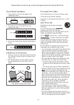
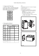
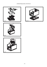
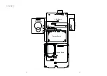
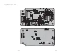
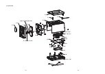
Page 24: ...8 2 Fig D3 Fig D5 Fig D4 Cabinet Disassembly Instructions Fig D6 A02 A03 A04 A02 ...

Page 25: ...d circuit check and change the related components of radio controlled circuit check if power supply of radio is normal check and change related components of power supply circuit check if radio circuit components of around it is normal check and change components of around it No No No No No No No sound from whole unit FLOW CHART NO 3 Yes No Yes No Yes no sound from DVD check if DVD output is norma...

Page 26: ... wire is broken check and change video wire socket No display from display screen check if video socket video wire is normal Decoding is broken check if tie wires of laser head ass y is loosen and broken laser head ass y broken no image from DVD change capacitance change display screen check if display screen is broken Yes check if the capacitor voltage of filaments filter is short circuit Yes che...

Page 27: ...09 IIC LED BUS Stb clk data Seg grid BUS MCU3 3V M3 3V AMP VDD M3 3V BD3491 3490 OPT 4558 5V BD3490FS FR_OUT AMPLIFIER TDA7491HV FL_OUT MCU R5F21266 IR IR AD_KEY EEPROM M24C02 STB MUTE STB MUTE TX RX CTL DET KEY 9 6OHM_5W 2 TX RX CTL DET DVD_ON VUSB_ON DC DC AP1538 9435 DVD_5V 12V 18V AMP TDA7491HV S3 3V F3 3V E3 3V TRANSFORMER AC220V CD DVD_ON GND IGND I5V 3 3V 1117 LDO 7333 MCU3 3V M3 3V ECO IPO...

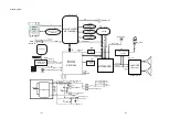
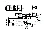
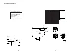
Page 28: ...Wiring Diagram Display Board Decoder Board AMP Board DVD Loader Power Board 11 1 11 1 ...

Page 29: ...19 CB95 0 1uF R187 8 2R R134 4 7K C47 0 47uF TP18 C122 4 7uF R108 10K CE27 220uF 16V TP39 CB89 2 2u R92 10K R188 100R CE35 1000uF 35V CE26 220uF 16V C128 100pF L49 FB 0603 2 2K R297 100K NC J4 RF IN 3 2 1 4 6 7 5 D38 BAS316 NC L77 FB 33 C136 4 7uF R98 0R L14 0 NC R68 FB1K NC R297 100K C114 104 C110 100pF CB75 0 1uF CB81 0 1UF TP33 C77 3300pF L53 FB 0603 2 2K CB65 1000pF TP35 L45 FB 0603 2 2K C118 ...

Page 30: ...00u 10V U16 AMS1117 3 3 SOT223 1 3 4 2 ADJ IN OUT2 OUT1 R249 47K R241 4 7K R253 4 7K 1 Q35 CES2307 SOT23A 1 2 3 C139 NS 100nF R254 24 9k 1 C137 0 1uF C142 10u 10V Q34 CES2307 SOT23A 1 2 3 R259 0R TP44 C134 0 1uF Q30 BS3904 1 3 2 L70 FB_0349 TP46 U17 AP1538 SOP 8 SOP8 SMD 1 2 3 4 5 6 7 8 FB EN OCSET Vcc O P O P Vss Vss R252 22K CE52 220u 25V D25 SK34 CE45 100u 10V TP52 L71 47UH 3A L66 DCR 33R TP45 ...

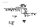
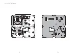
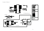
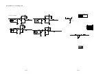
Page 31: ...AMP Board Layout Diagram 12 3 12 3 ...

Page 32: ...3 SG4 SG5 SG6 SG7 SG8 SG9 SG10 SG11 SEG00 SEG08 SEG09 SEG10 SEG11 SEG12 SEG13 SEG14 SEG15 SEG16 SEG17 SEG18 SEG19 SEG20 SEG21 SEG22 SEG23 SEG07 SEG06 SEG05 SEG04 SEG03 SEG02 SEG01 SEG00 COM07 COM06 COM05 COM04 COM03 COM02 COM01 COM00 COM8 COM7 COM6 COM5 COM4 COM3 COM2 COM1 SEG8 SEG7 SEG6 SEG5 SEG4 SEG3 SEG2 SEG1 SEG16 SEG15 SEG14 SEG13 SEG20 SEG21 SEG22 SEG23 32 31 30 29 28 27 26 25 24 23 22 21 20...

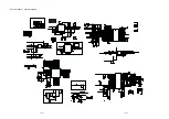
Page 33: ...Display Board Layout Diagram 12 5 12 5 ...

Page 34: ... R19 2 32K 1 0805 R5 2M 1206 D4 1N4007 R7 NC C6 2200uF 10V D11 NC R10 1 2R 1206 R3 2M 1206 D5 NC D6 FR107 R16 3 3K 0805 C2 22uF 50V C1 47uF 400V C3 103P 630V C11 470pF 0805 D7 FR107 R18 12K R13 68R 0805 Q1 4N60 C21 1nF 50V 0805 D9 SB3100 R1 200K 1206 C4 221P 2KV R28 NC R25 330R 0805 C13 NC 1 2 L2 0R 0805 L3 NC IC3 NC SOT23 R23 NC R12 1K 0805 RT 3 CS 4 GND 1 OUT 6 VCC 5 FB 2 IC4 KB8235 SOT23 6 R22 ...

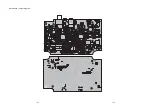
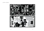
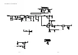
Page 35: ...Power Board Layout Diagram 12 7 12 7 ...

Page 36: ... AKIN1 TRCLOSE TRIN UP1_6 UP1_7 94 95 VSCK VSDA MS_CLK GPIO20 GPIO21 107 108 97 106 AUDIO_MUTE GPO14 GPIO19 SCART1 SCART2 VSTB MT1389J General GPIO List Gxyz_CLK MS_BS MS_D0 SD_CLK SD_CMD SD_D0 LIMIT Gxyz_DA1 Gxyz_DA2 VSYNC HSYNC Gxyz_LOAD RXD GPIO3 STBY TROPEN IOA GPIO30 GPIO31 GPIO10 GPIO33 GPI36 124 TXD AKIN2 Power Key R3 10K R1 0R MARK4 CB3 0 1uF CB2 0 1uF MARK2 2 2 3 3 4 4 5 5 9 9 8 8 7 7 6 6...

Page 37: ...32 47K C17 4 7uF R26 27k R16 56R 2 1 3 Q3 SS8550 SOT23 D CB5 0 1uF CB16 0 1uF R18 4 7R R28 15k C25 NC 0 015uF C8 27pF R12 4 7k TP47 R8 100k CB4 0 1uF 1 2 3 4 CON7 PBZ DVD Y TP6 TP49 R13 100R C2 0 1uF CB19 0 1uF 1 2 3 4 J2 4P 2 0MM C9 0 1uF L6 10uH TP5 TP50 CB11 0 1uF CB9 0 1uF L4 FB CB10 0 1uF TP4 TP51 C21 0 015uF C24 NC 0 015uF 100R R14 TP12 R6 10k CB13 0 1uF R39 10K 2 1 3 Q2 SS8550 SOT23 D CE10 ...

Page 38: ...2V output AM5888 AT5669 R44 10k CB23 0 1uF D3 IN4001 CE13 100uF 16v CE15 100uF 16v 2 1 3 Q7 SS8550D TO 92A CB27 0 1uF CB26 0 1uF R40 10k R45 10k R42 33R R51 10k CB20 0 1uF R41 10k L13 33R R47 20k CB24 0 1uF CB21 0 1uF R49 12k L12 FB C26 10pF NC D5 IN4001 CB22 0 1uF CE51 220uF 16v L14 FB 2 1 3 Q6 SS8550D TO 92A CE14 100uF 16v R50 10k CE 1 SO 2 WP 3 VSS 4 SI 5 SCK 6 HOLD 7 VDD 8 U4 MX25L3206E CB25 0...

Page 39: ...0R 2 1 3 Q10 2N3904 C32 47pF C30 47pF C28 47pF CE16 CD11X 100uF16V 2 1 3 Q9 2N3904 R61 3 3K C35 47pF L67 FB CB30 0 1uF L15 FB L20 FB 0603 C29 47pF CB29 0 1uF 2 1 3 Q11 2N3904 CE19 CD11X 22UF16V 1 2 3 4 5 6 7 8 9 10 CON6 10pin 2 0 CON2 0 10 CB31 0 1uF CE17 CD11X 22UF16V CE18 CD11X 22UF16V D4H7 R56 2 2K R62 160R CE20 CD11X 22UF16V R58 75 1 C36 0 1uF R52 3 3K R63 2 2K R57 2 2K R68 100R R244 62R R54 1...

Page 40: ...TP10 R202 470K NC R197 0R R145 10K CE25 220uF 16V CE25 220uF 16V C89 1uF CB41 NC 33PF R174 5 6k C45 680pF C119 100pF 2 1 3 NC 8050 DIP Q19 R162 330R TP22 L25 0603 0 27uH 催乥催Q 100MHz Qؐ Ѣ25 TP11 CE33 1u 50V R117 NC 10K C141 4 7uF R71 1K R185 NC 3R3 Y2 32 768KHz C47 0 47uF TP19 R187 8 2R CB95 0 1uF R134 4 7K TP13 CE27 220uF 16V C122 4 7uF R131 15K R108 10K TP18 C90 1uF R92 10K R217 470R R192 100R CB...

Page 41: ...0R R234 1K TP45 C139 NS 100nF R252 22K R260 0 L70 FB_0349 GND 1 IN 2 OUT1 3 U14 NC HT7333 SOT89 CE41 100u 16V R241 4 7K L71 47UH 3A 1 3 2 Q25 BS3904 1 2 3 4 5 CON2 5 5 CON2 54 5 CON5 R255 4 7K R239 33K CE45 100u 10V TP52 R242 22K 1 2 3 Q35 CES2307 SOT23A FB 1 EN 2 OCSET 3 Vcc 4 O P 5 O P 6 Vss 7 Vss 8 U17 AP1538 SOP 8 SOP8 SMD R247 0 ADJ 1 IN 3 OUT2 4 OUT1 2 U16 AMS1117 3 3 SOT223 1 2 3 Q34 CES230...

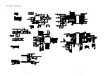
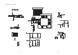
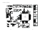
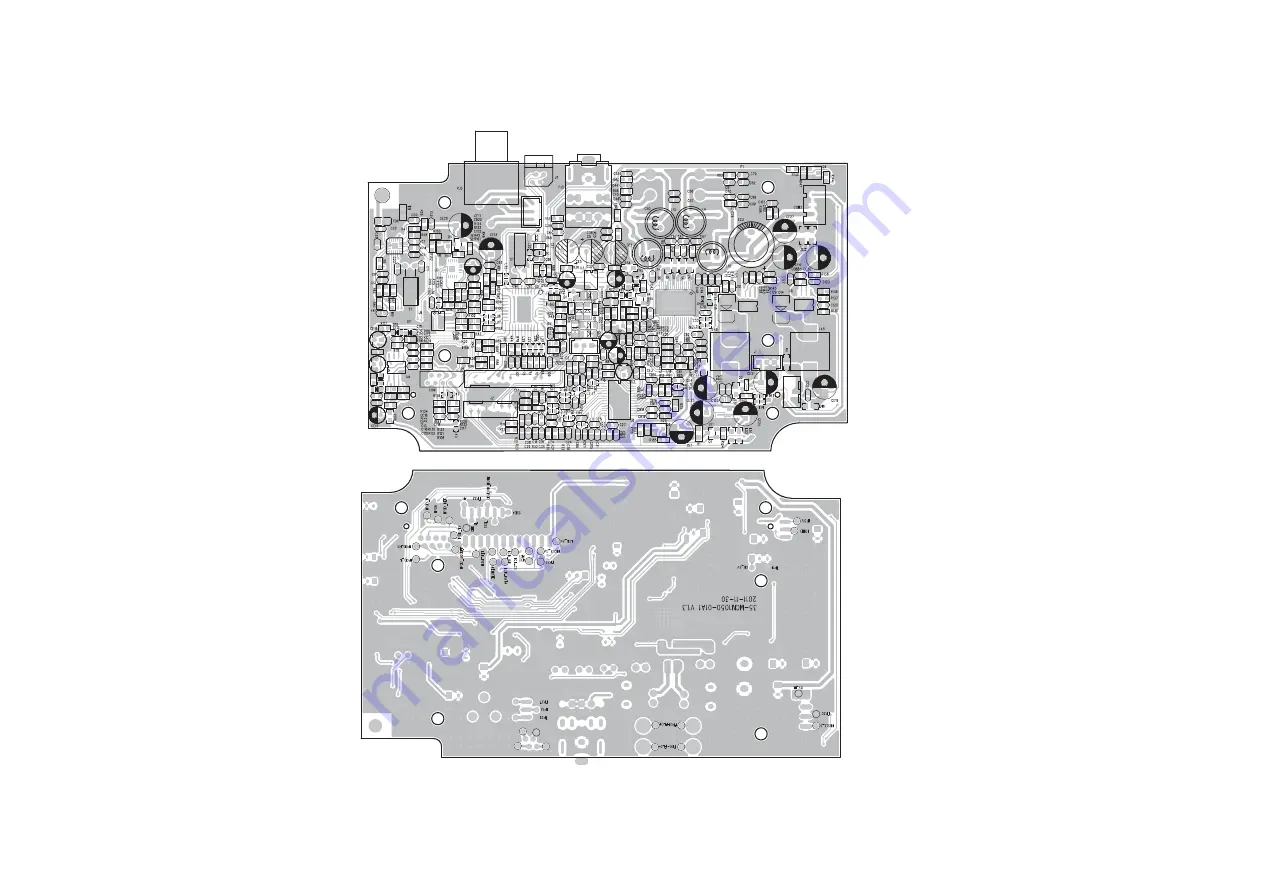
Page 42: ...Decoder Board Layout Diagram 12 14 12 14 ...

Page 43: ...iew S107 S104 S110 S109 Screw Gear Bracket CD Door Gear CDM Screw Screw Screw Screw PCB1 PCB3 S100 Bottom Cover Rubber Foot PCB4 PCB2 S108 S106 S101 S105 S111 Light Guide Ringe PMMA IR Receiver Bracket 13 1 13 1 ...

Page 44: ...Revision List Revision List Version 1 0 Initial Release 14 1 ...

Reviews: