background image

6-1

6-1

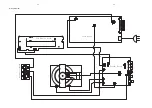
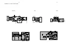
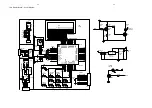
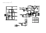
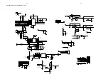
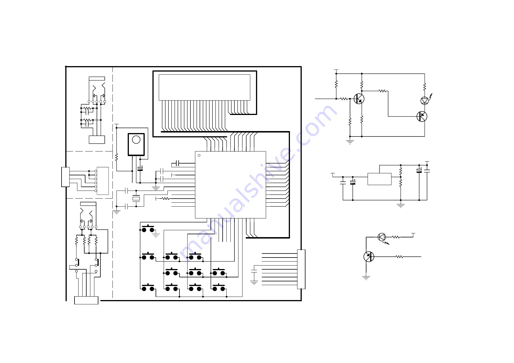
LCD Display Board -- Circuit Diagram

C1005

104

C1003

104

C1004

104

3V

X1000

32.768

C1008

15P

C1009

15P

3V

R1012

30K

SW1001

|<<

SW1002

open/close

SW1003

standby

SW1007

volume-

SW1009

stop

SW1011

mode

SW1006

SW1008

>>|

SW1010

source

SW1012

play

SW1000

DBB

5V

GND

SDA

ECO_POWER

SCL

ECO_POWER

MUTE

IR

REM

1

GND

2

Vcc

3

S1000

REMOTE

C1002

47U/6.3V

R1006

4.7K

5V

IR

1

2

3

4

5

6

7

8

9

CN1002

8P

IR

K3

K2

K1

K0

KS2

KS1

KS0

vbus

1

D-

2

D+

3

GND

4

Shield

5

GND

6

J1001

USB

GND

D+

D-

VBUS

1

2

3

4

CN1000

4PIN/2.0

C1014

104

LCD

1 2 3 4 5 6 7 8 9 10 11 12 13 14 15 16 17 18 19 20 21 22 23 24 25 26 27 28

U1000

LCD

seg21

seg1 seg2 seg3 seg4 seg5 seg6 seg7 seg8 seg9 seg10 seg11 seg12 seg13 seg14 seg15 seg16 seg17 seg18 seg19 seg20

com1 com2 com3 com4 com5 com6 com7

com1

com2

com3

com4

com5

com6

com7

seg1 seg2 seg3

seg5 seg6

seg7

seg8

seg9

seg10

seg11

seg12

seg13

seg14

seg15

seg16

seg17

seg18

seg

19

seg

20

seg

21

LED

cup2

1

cup1

2

VDD3

3

VDD

4

VDD1

5

GND

6

XOUT

7

XIN

8

STB

9

OSCIN

10

CLK

11

IR

12

K3

13

K2

14

K1

15

K0

16

STANDBY

17

MUTE

18

DATA

19

KS2

20

KS1

21

KS0

22

SEG21

23

SEG20

24

SEG19

25

SEG18

26

SEG17

27

SEG16

28

SEG15

29

SEG14

30

SEG13

31

SEG12

32

SEG11

33

SEG10

34

SEG9

35

SEG8

36

SEG7

37

SEG6

38

SEG5

39

SEG4

40

SEG3

41

SEG2

42

SEG1

43

COM1

44

COM2

45

COM3

46

COM4

47

COM5

48

COM6

49

COM7

50

U1001

ZX935P

seg4

K0

MUTE handshake

SDA

SCL

1

2

3

4

5

CN1003

4PIN/2.0

J1002A

J1002C

J1002B

PGND

H_OUTR

H_OUTL

J1000A

MP3 IN

1

2

3

CN1001 2.0/3P

headphone

AGND

MP3_L

MP3_R

R1000

47K

R1005 47K

C1000

100P

C1001

100P

R1010

47K

R1011

47K

R101

100

R100

100

LED1000

white

LED

Q1000

8050

R1002
4.7K

5V

LED

LED1001

blue LED

R1008
2.2k

R1013
1.2K

5V

ECO_POWER

R1001

10K

R1003

4.7K

R1004
10

R1009

100

R1007

2K

GND

1

OUT

2

IN

3

IC1000

1117-ADJ

C1010

104

C1011

220U/16V

5V

R1014

750

R1015

1.2k

C1012

100U/16V

C1013

104

3V

Q2

8550

Q1

PNP

R1020

56

H_IN

H_IN

GND

Summary of Contents for MCD122

Page 1: ...are Version Check Upgrade 2 1 Malfuction Check Chart 2 2 Disassembly Diagram 3 1 Block Diagram 4 1 Wiring Diagram 4 2 Small Board 5 Circuit diagram 5 1 Layout diagram 5 1 LCD Display Board 6 Circuit diagram 6 1 Layout diagram 6 2 Power Board 7 Circuit diagram 7 1 to 7 2 Layout diagram 7 3 Decoder Board 8 Circuit diagram 8 1 to 8 4 Layout diagram 8 5 Exploded View 9 1 Service Partlist 10 1 to 10 2 ...

Page 2: ...ARD DECODER BOARD TIPS C Component Level Repair M Module Level Repair Used 55 55 58 58 61 61 79 79 93 93 94 94 96 96 98 98 37 37 12 12 05 05 Feature diffrence RDS TDS VOLTAGE SELECTOR ECO STANDBY DARK C M M M Type Versions MCD122 AMP Power Board Decoder Board Scart Board LCD Display Board USB Headphone Board 1 1 SCART BOARD C M M M M C M M M ...

Page 3: ...dB Total Harmonic Distortion 3 Signal to Noise Ration 50dBA SPEAKERS Speaker Impedance 2x8ohm e Speaker Driver base 4 Speaker Driver tweeter Buzzer Frequency Response 100Hz 5dB 5 15KHz GENERAL INFORMATION Total Output power 40W RMS AC Power 220V 50Hz Operation Power Consumption 40W Standby Power Consumption 6W Eco Standby Power Consumption 1W Headphone Output 500mV 32ohm USB Direct Version 2 0 Dim...

Page 4: ...15kHz e g 7122 707 48001 LF Voltmeter e g PM2534 DUT S N and distortion meter e g Sound Technology ST1700B Frame aerial e g 7122 707 89001 Tuner AM MW LW To avoid atmospheric interference all AM measurements have to be carried out in a Faraday s cage Use a bandpass filter or at least a high pass filter with 250Hz to eliminate hum 50Hz 100Hz RF Generator e g PM5326 Ri 50 Bandpass 250Hz 15kHz e g 71...

Page 5: ...ng make sure that you are connected with the same potential as the mass of the set via a wrist wrap with resistance Keep components and tools also at this potential ESD CLASS 1 LASER PRODUCT GB Safety regulations require that the set be restored to its original condition and that parts which are identical with those specified be used Safety components are marked by the symbol Lead free ...

Page 6: ...ET OK check playability N Y playability ok check playability check playability return set Customer complaint CD related problem fast lens cleaning 1 2 3 For flap loaders access to CD drive possible cleaning method 4 is recommended INSTRUCTIONS ON CD PLAYABILITY 1 Exchange CDM 1 4 For description see following pages ...

Page 7: ...obviously caused by a scratched dirty or copy protected CD In case problems remain the customer is requested to contact the workshop directly The lens cleaning method 3 should be mentioned in the addendum sheet The final wording in national language as well as the printing is under responsibility of the Regional Service Organizations 4 LIQUID LENS CLEANING Because the material of the lens is synth...

Page 8: ...s press the SYSTEM MENU on remote control TV Screen Display Upgrading Software Upgrade Erasure and Upgrade OK Cancel Software Upgrade Upgrading Please don t remove the player power Door Open OR 1 Download the software from Philips support website 2 Load the CD Disc or USB device with software Software upgrade procedure starts automatically Waiting a minute VFD Display TV Screen Display Software up...

Page 9: ...Plug in the power cord Reset the Time Clock Replace a new Power Board Check if the USB or other devices are connected Check if the USB or other devices are incompatible Check the data wire which connected the Main Board if has provided voltage Check if there is voltage supplied to the USB Board Check if the CPU IC has provided voltage Check if the VFD Board has provided voltage No Replace a new on...

Page 10: ...C2 Loose 1pc screw 3 x 8 BA E Remove Decoder Board E1 Loose 4pcs screws 3 x 10 FA of the back side E2 Loose 2pcs screws 3 x 10 FA of the decoder board D Loose 4pcs screws 3 x 10 PWA to remove DVD Loader Driver F Loose 2pcs screws 3 x 8 FT to remove the Front Cabinet G Loose 1pc screw 3 x 8 BA to remove the Headphone Board A Open the DVD Door and loose 2 clipps to remove the door H Remove the Displ...

Page 11: ...PK Door Detect DISPLAY BOARD MAIN BOARD or Si4705 RDS MCU I2C M3 3V FM RST FM RST STANDBY ECO_POWER ECO_POWER 1 2 1 2 TDA1517 POWER AMP F4558 PWM 15V AUDIO ML MR FL FR CLOSE DOOR OPEN DOOR Y U V S VIDEO COAXIAL MCU5V MCU I2C MPEG I2C FM RST STANDBY ECO_POWER MPEG I2C MCU5V MCU5V MUTE 4052 A B 5W 5W AV POWER MUTE STANDBY M3 3V M1 8V M5V 8550 POWER1 FL FR EEPROM M3 3V AT24C02 1M 16 AT26DF081A IPOD D...

Page 12: ...4 2 4 2 Wiring Diagram Power Board Decoder Board LCD Display Board Headphone USB Board DVD Loader Driver ...

Page 13: ... 5 GND 6 J1001 USB GND D D VBUS 1 2 3 4 CN1000 4PIN 2 0 1 2 3 4 5 CN1003 4PIN 2 0 J1002A J1002C J1002B PGND H_OUTR H_OUTL J1000A MP3 IN 1 2 3 CN1001 2 0 3P headphone AGND MP3_L MP3_R R1000 47K R1005 47K C1000 100P C1001 100P R1010 47K R1011 47K R101 100 R100 100 H_IN H_IN ...

Page 14: ...eg8 seg9 seg10 seg11 seg12 seg13 seg14 seg15 seg16 seg17 seg18 seg19 seg20 seg21 LED cup2 1 cup1 2 VDD3 3 VDD 4 VDD1 5 GND 6 XOUT 7 XIN 8 STB 9 OSCIN 10 CLK 11 IR 12 K3 13 K2 14 K1 15 K0 16 STANDBY 17 MUTE 18 DATA 19 KS2 20 KS1 21 KS0 22 SEG21 23 SEG20 24 SEG19 25 SEG18 26 SEG17 27 SEG16 28 SEG15 29 SEG14 30 SEG13 31 SEG12 32 SEG11 33 SEG10 34 SEG9 35 SEG8 36 SEG7 37 SEG6 38 SEG5 39 SEG4 40 SEG3 4...

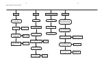
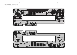
Page 15: ...6 2 6 2 LCD Display Board Layout Diagram ...

Page 16: ...1 50V C19 471 50V R21 100K 1 0805 CY1 332 250V C44 104 50V 0805 NC R27 10K 1206 IC4 TL431A Q3 D882 Q4 S8050 R17 5 1K 0805 Q1 FQPF8N60 C4 22uF 35V R15 1M 1206 R12 1M 1206 D2 1N5408 D1 1N5408 LT2 2 5MH T18 LT1 30MH UU10 5 F1 T3 15A 250V RT1 MF72 10D 9 D3 1N5408 D7 1N5408 R20 750K 1206 C2 103 630V D5 FR157 D130 NC R280 C21 1000uF 10V R19 330R 1W R18 5 1K 0805 R38 100K 0805 R25 3 3K 5 0805 R79 33R 1W ...

Page 17: ...18V Q8 MMET2222 Q9 MMET2222 DZ2 12V Q2 MMBT2222 FRIN MUTE1 STANDBY D12 1N4148 D15 1N4148 MUTE1 MUTE HP MUTE R32 10K 1206 C7 1uF 50V Q5 MMBT2222 Q6 MMBT2222 C31 47uF 16V C30 1uF 25V R56 4 7K 1 4W R55 4 7K 0805 C32 1uF 25V R54 100K 0805 C35 220uF 16V CON4 2 0 4P Q11 9014 C33 1uF 25V C36 220uF 16V VCC R59 10K 0805 R53 22K 0805 S08 PT2309 R23 10K 0805 R45 10K 0805 TDA8948J R41 1 5K 0805 R49 10K 1206 C...

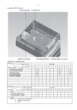
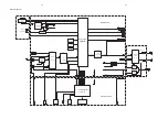
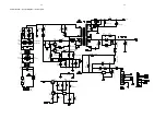
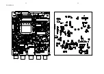
Page 18: ...Power Board Layout Diagram 7 3 7 3 ...

Page 19: ... VDD 8 C11 10nF C11 10nF EC23 100uF 10V EC23 100uF 10V C47 10nF C47 10nF C12 10nF C12 10nF PH1 PH1 1 FB6 MBW2012 221 FB6 MBW2012 221 R117 100R R117 100R R4 15 4K 1 R4 15 4K 1 C1 10nF C1 10nF C134 100pF C134 100pF C25 1nF C25 1nF C40 10nF C40 10nF FB7 MBW2012 221 FB7 MBW2012 221 EC5 100uF 10V EC5 100uF 10V U2A U2A Gen_5 GPIO 0 102 Gen_6 101 GPIO 52 PWMCO 3 HSYNC 93 GPIO 51 PWMCO 2 FIELD 92 GPIO 50 ...

Page 20: ...2 OUTSW 3 GND 4 INSW 5 TP23 TP23 EC6 220uF 6 3V EC6 220uF 6 3V L1 10uH L1 10uH R51 33R R51 33R TP6 TP6 TP12 TP12 R48 2K R48 2K Q2 BT2907 Q2 BT2907 1 2 3 D1 BAT54C D1 BAT54C 2 3 1 TP13 TP13 TP24 TP24 C54 NM 470pF C54 NM 470pF C62 0 1uF C62 0 1uF C73 0 1uF C73 0 1uF CN3 24Pin OPU connector CN3 24Pin OPU connector GND LD 24 DVD LD 23 NC 22 HFM 21 MD 20 CD LD 19 VR DVD 18 VR CD 17 NC 16 E 15 VCC 14 VC...

Page 21: ...NNA_1 C130 10uF 0805 C130 10uF 0805 C106 22pF C106 22pF C100 0 1uF C100 0 1uF R75 82K R75 82K R172 4 7K R172 4 7K FB23 FB 2K FB23 FB 2K C104 0 1uF C104 0 1uF R118 100K R118 100K C110 0 1uF C110 0 1uF D8 1N4148 D8 1N4148 1 2 R377 NC 1K R377 NC 1K R168 4 7K R168 4 7K U5A CF4558 U5A CF4558 3 2 1 8 4 J5 DASW 02 9 J5 DASW 02 9 14 13 12 11 10 5 4 3 1 9 2 6 8 7 R69 1K R69 1K R104 10R R104 10R J3 NC J3 NC...

Page 22: ... C81 0 1uF C81 0 1uF EC13 47uF 16V EC13 47uF 16V D402 BAT54S D402 BAT54S 2 3 1 C113 10nF C113 10nF R392 330R 0 5W R392 330R 0 5W FB408 1K FB408 1K C410 22pF C410 22pF C125 NC 100pF C125 NC 100pF C122 NC 100pF C122 NC 100pF MARK3 1 Q11 AO3407 Q11 AO3407 R433 2 2K R433 2 2K C133 NC 100pF C133 NC 100pF FB21 FB 0805 FB21 FB 0805 C425 150pF C425 150pF D403 BAT54S D403 BAT54S 2 3 1 R95 10K R95 10K Q313 ...

Page 23: ...8 5 8 5 Decoder Board ...

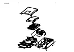
Page 24: ...9 1 9 1 Exploded View ...

Page 25: ...3 DVD FRONT CABINET HIPS D004 996510025539 MCD113 FUNCTION BUTTON ABS D005 996510025534 MCD113 DIRECTION BUTTON ABS D006 996510025529 MCD113 CENTER BUTTON ABS D008 996510025549 MCD113 FUNCTION BUTTON L ABS D009 996510025546 MCD113 FUNCTION BUTTON R ABS D009 996510025546 MCD113 FUNCTION BUTTON R ABS D022 996510025552 MCD113 DVD TOP COVER HIPS D023 996510025649 MCD113 DVD BOTTOM CHASSIS HIPS 12 D023...

Page 26: ...00263 LIGHT TOUCH SWITCH 6X6X5 SW2 996510000263 LIGHT TOUCH SWITCH 6X6X5 SW3 996510000263 LIGHT TOUCH SWITCH 6X6X5 SW4 996510000263 LIGHT TOUCH SWITCH 6X6X5 SW5 996510000263 LIGHT TOUCH SWITCH 6X6X5 SW6 996510000263 LIGHT TOUCH SWITCH 6X6X5 SW7 996510000263 LIGHT TOUCH SWITCH 6X6X5 SW8 996510000263 LIGHT TOUCH SWITCH 6X6X5 SW9 996510000263 LIGHT TOUCH SWITCH 6X6X5 U1 996510024049 LCD DRIVER MODUL ...

Page 27: ...H C 5 C R 7 X 5 0 8 0 K V 0 5 p 4 0 1 P A C P I H C 6 C R 7 X 5 0 8 0 K V 0 5 p 4 0 1 P A C P I H C 7 C R 7 X 5 0 8 0 K V 0 5 p 4 0 1 P A C P I H C 8 C R 7 X 5 0 8 0 K V 0 5 p 4 0 1 P A C P I H C 9 C R 7 X 5 0 8 0 K V 0 5 p 4 0 1 P A C P I H C 0 1 C R 7 X 5 0 8 0 K V 0 5 p 4 0 1 P A C P I H C 3 1 C 6 X 4 5 M V 3 6 u 7 4 P A C C I T Y L O R T C E L E 3 C 7 X 5 5 L V 0 1 u 0 0 1 P A C C I T Y L O R ...

Reviews: