background image

Version 1.0

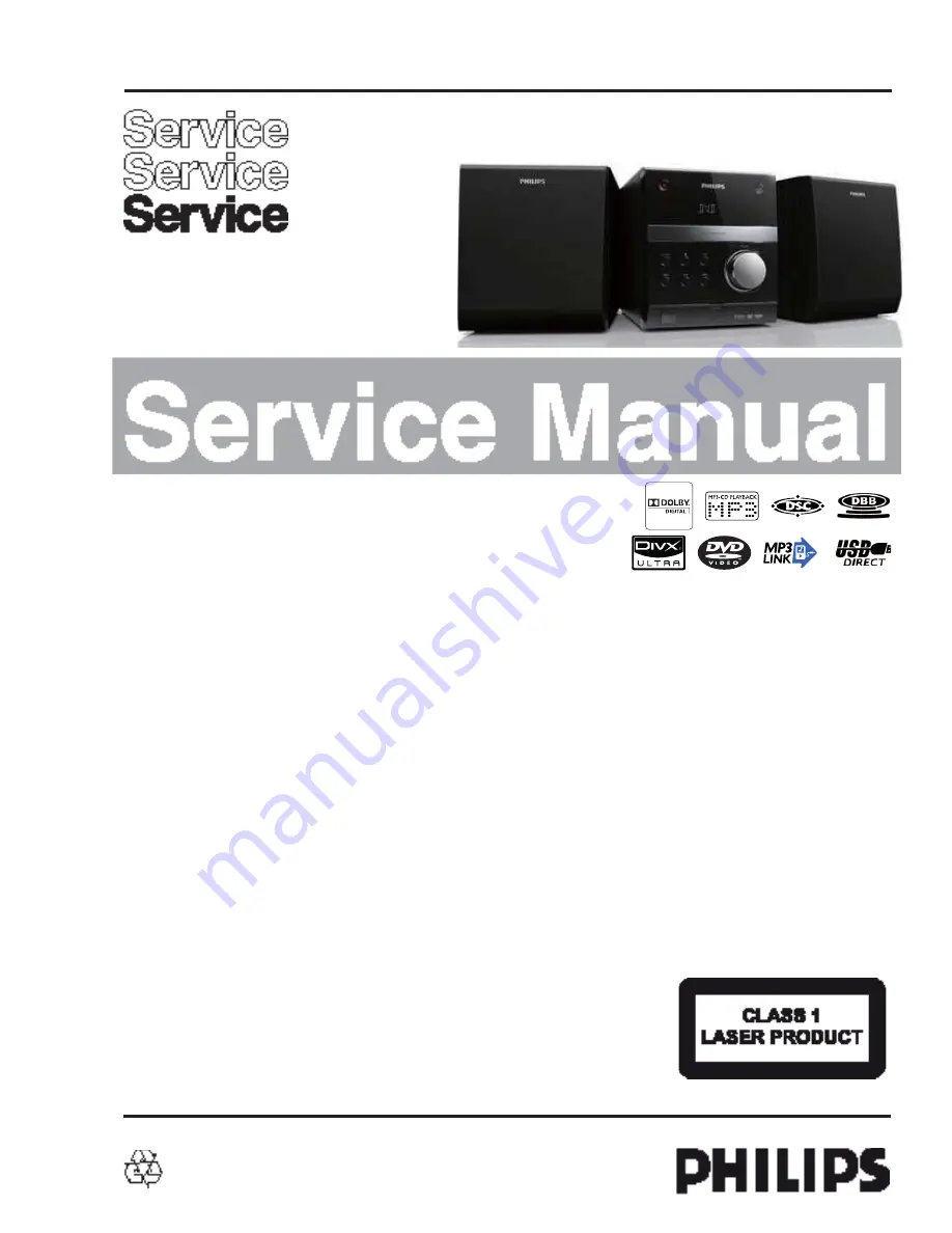
MCD135

 3141 785 35670

50W Classic DVD Micro System

-/78/51/58/55

Published by SW 1046 Service Audio    Subject to modification

© 

Copyright 2010 Philips Consumer Electronics B.V. Eindhoven, The Netherlands

All rights reserved. No part of this publication may be reproduced, stored in a retrieval
system or transmitted, in any form or by any means, electronic, mechanical, photocopying,
or otherwise without the prior permission of Philips.

CONTENTS

Technical specification and version variation ...............................1-2

Service measurement setup..........................................................1-3
Service aids  .................................................................................1-4

Instructions on CD playability ...............................................2-1.. 2-2

Block diagram ................................................................................3-1
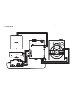
Wiring diagram ..............................................................................4-1
Disassembly diagram..............................................................4-2..4-3 

Main board and Tuner board
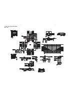
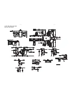
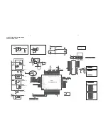
          Circuit  diagra......................................................................5-1..5-6            
     Layout diagram .........................................................................5-7

Display and Key board
     Circuit diagram ..................................................................6-1..6-2 
     Layout diagram ..................................................................6-3..6-4

SMPS Power board
     Circuit diagram .........................................................................7-1 
     Layout diagram ..................................................................7-2..7-3

Exploded view diagram .................................................................8-1

Summary of Contents for MCD135

Page 1: ...by any means electronic mechanical photocopying or otherwise without the prior permission of Philips CONTENTS Technical specification and version variation 1 2 Service measurement setup 1 3 Service aids 1 4 Instructions on CD playability 2 1 2 2 Block diagram 3 1 Wiring diagram 4 1 Disassembly diagram 4 2 4 3 Main board and Tuner board Circuit diagra 5 1 5 6 Layout diagram 5 7 Display and Key boar...

Page 2: ... dBf Search Selectivity 28dBf Total Harmonic Distortion 2 Signal to Noise Ratio 55dB Speakers Speaker Impedance 6 ohm Speaker Driver Full range speaker Sensitivity 80 dB m W 4dB m W General information AC power 110 240 V 50 60 Hz Operation Power Consumption 25 W Eco Standby Power Consumption 1 W Composite Video Output 1 0 Vp p 75 ohm Headphone output 2 X 15 mW 32 ohm USB Direct Version 2 0 Dimensi...

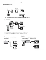
Page 3: ...15kHz e g 7122 707 48001 LF Voltmeter e g PM2534 DUT S N and distortion meter e g Sound Technology ST1700B Frame aerial e g 7122 707 89001 Tuner AM MW LW To avoid atmospheric interference all AM measurements have to be carried out in a Faraday s cage Use a bandpass filter or at least a high pass filter with 250Hz to eliminate hum 50Hz 100Hz RF Generator e g PM5326 Ri 50 Bandpass 250Hz 15kHz e g 71...

Page 4: ...ng make sure that you are connected with the same potential as the mass of the set via a wrist wrap with resistance Keep components and tools also at this potential ESD CLASS 1 LASER PRODUCT GB Safety regulations require that the set be restored to its original condition and that parts which are identical with those specified be used Safety components are marked by the symbol Lead free ...

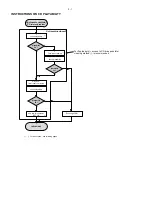
Page 5: ...T OK check playability N Y playability ok check playability check playability return set Customer complaint CD related problem fast lens cleaning 1 2 3 For flap loaders access to CD drive possible cleaning method 4 is recommended INSTRUCTIONS ON CD PLAYABILITY 2 1 Exchange CDM 1 4 For description see following pages ...

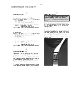
Page 6: ...viously caused by a scratched dirty or copy protected CD In case problems remain the customer is requested to contact the workshop directly The lens cleaning method 3 should be mentioned in the addendum sheet The final wording in national language as well as the printing is under responsibility of the Regional Service Organizations 4 LIQUID LENS CLEANING Because the material of the lens is synthet...

Page 7: ...SET BLOCK DIAGRAM 3 1 3 1 ...

Page 8: ...SET WIRING DIAGRAM 4 1 4 1 ...

Page 9: ...5 1 5 1 CIRCUIT DIAGRAM MAIN BOARD MCU PART ...

Page 10: ...5 2 5 2 CIRCUIT DIAGRAM MAIN BOARD AUDIO AND POWER PART ...

Page 11: ...5 3 CIRCUIT DIAGARM MAIN BOARD POWER AMP PART 5 3 ...

Page 12: ...C 2 1 3 4 C965 100pF C965 100pF C966 1000pF C966 1000pF R962 4 7K1 R962 4 7K1 R964 75R1 R964 75R1 R973 10K R973 10K R961 10K R961 10K C963 100pF C963 100pF C960 100pF C960 100pF R976 100 R976 100 FB982 FB 0805 FB982 FB 0805 EC924 10uF16V EC924 10uF16V EC926 100uF16V EC926 100uF16V R967 27K1 R967 27K1 R972 75R1 R972 75R1 D909 BAV99 D909 BAV99 C967 1000pF C967 1000pF D910 BAV99 D910 BAV99 Q914 2N390...

Page 13: ...79 CDLDO 103 DVDMDI 104 CDMDI 105 SRV_AVDD 106 V21 107 V165 108 DA_AVSS 109 DA_TEO 110 DA_FEO 111 DA_AVDD 112 SPDC_OUT 113 SC_OUT 114 DVDVR 115 DMEA 116 SD_D1 GPIO4 117 SD_D0 GPIO5 118 SD_CLK GPIO6 119 TRAYIN SD_SMD GPIO7 120 TRAYOUT SD_D3 GPIO8 121 SD_D2 GPIO9 122 CDVR 123 SPI_CE 124 SPI_D0 125 SPI_CLK 126 SPI_D1 127 ADAC_AVSS 64 VREF 61 ADAC_AVDD 62 AOUT_RS 59 AOUT_LS 60 ADAC_AVSS 58 AOUT_SUBW 5...

Page 14: ...1 L905 10uH L905 10uH C908 0 1uF C908 0 1uF Q910 2SB1132 R type Q910 2SB1132 R type Q909 2SB1132 R type Q909 2SB1132 R type 6PIN 2 0mm XP902 6PIN 2 0mm XP902 1 2 3 4 5 6 L904 10uH L904 10uH R922 5 1 R922 5 1 0 1uF BC908 0 1uF BC908 D903 1N4001 D903 1N4001 Q903 B772 Q903 B772 2 1 3 EC915 100uF 16V EC915 100uF 16V C903 0 1uF C903 0 1uF 0 1uF BC907 0 1uF BC907 R905 NC R905 NC 0 1uF BC912 0 1uF BC912 ...

Page 15: ...LAYOUT DIAGRAM MAIN BOARD 5 7 5 7 ...

Page 16: ...CIRCUIT DIAGRAM DISPLAY AND KEY BOARD PART 1 6 1 6 1 ...

Page 17: ...CIRCUIT DIAGRAM DISPLAY AND KEY BOARD PART 2 6 2 6 2 ...

Page 18: ...LAYOUT DIAGRAM DISPLAY AND KEY BOARD TOP SIDE 6 3 6 3 ...

Page 19: ...LAYOUT DIAGRAM DISPLAY AND KEY BOARD BOTTOM SIDE 6 4 6 4 ...

Page 20: ...CIRCUIT DIAGRAM SMPS POWER BOARD 7 1 7 1 ...

Page 21: ...LAYOUT DIAGRAM SMPS POWER BOARD TOP SIDE 7 2 7 2 ...

Page 22: ...LAYOUT DIAGRAM SMPS POWER BOARD BOTTOM SIDE 7 3 7 3 ...

Page 23: ...EXPLODED VIEW DIAGRAM 8 1 8 1 134 133 SPK 126 130 128 127 106 105 119 125 123 124 103 117 120 109 111 110 107 114 112 115 121 108 113 118 122 101 116 ...

Reviews: