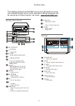
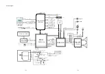
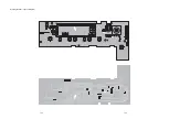
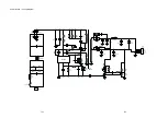
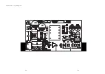
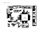
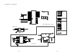
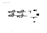
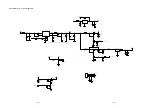
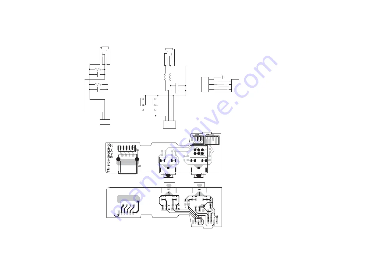
Headphone Board -- Circuit and Layout Diagram
1
2
4
3
5
PJ1
P
J
-C
K
3501
R1
47K
C1
103
1
1
2
2
3
3
CON1
CON2.0-3
2.0-3P
R2
47K
C2
103
FB
1
600R
FB
2
600R
1
1
2
2
3
3
4
4
CON3
C3
100P
C4
100P
1
3
2
11
10
PJ2
-A
J
P
-C
K
3511
PJ2
-B
PJ2
-C
MP
3_L
AGND
MP3_R
PGND
H_
OU
T
R
H_
OU
T
L
PH-MUTE
1
VCC
2
D-
3
D+
4
GND
USB
1
2
3
4
5
CON2
DGND
D+
D-
VBUS
12-1
12-1
Summary of Contents for MCD2010/12/93
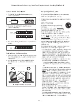
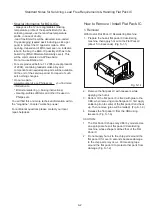
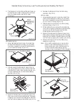
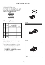
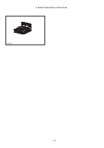
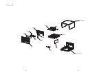
Page 26: ...8 2 Fig D4 Cabinet Disassembly Instructions ...
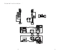
Page 33: ...Display Board Layout Diagram 12 3 12 3 ...
Page 35: ...Power Board Layout Diagram 12 5 12 5 ...
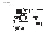
Page 42: ...Decoder Board Layout Diagram 12 12 12 12 ...
Page 44: ...Revision List Revision List Version 1 0 Initial Release 14 1 ...


