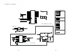
VIDEO I/F
OFF-PAGE CONNECTION
S-FLASH
DRAM I/F
AUDIO I/F
MCR I/F
I2C
Crystal
SERVO I/F
SERVO RF DeCAP.
RF Reference
VR-DVD
8
11
CD/DVD SW
20
A/a
23
1
NC
RF
15
18
D/d
F
7
T+
3
E
14
13
Vcc
GND-LD
12
Vc(Vref)
22
C/c
9
4
HFM
6
NC
CD-LD
2
16
VR-CD
DVD-LD
19
SANYO HD6x
GND-PD
F+
5
17
MD
24
10
B/b
F-
21
T-
Chip Decap.
RS-232
Default
Default
POWER
close to 89J IC
Gxyz
LD-CD
LD-DVD
LIMIT
V20
F-
F+
T+
T-
C
D
IOA
A
B
F
DCLK
MA[0..11]
SF_DI
DQ[0..15]
SF_CS
BA[0..1]
RAS#
SF_CK
SF_DO
DQM[0..1]
CAS#
WE#
MDI1
V1P4
STBY
TRIN
V_B
V_R
V_G
CVBS_OUT
F-
T+
SP+
SP-
SL-
SL+
F+
FOO
TRO
DMO
FMO
FOSO
DMSO
FMSO
TRSO
AL
AR
T-
RFO
V1P4
OPO
OP-
LDO2
TxD
RxD
DMSO
FMSO
TRSO
FOSO
SP-A
SP-
AVCC1
V20
E
AVCC1
1V2
URST#
RFO
XI
GPIO11
VR
_D
VD
VR
_C
D
XI
XO
XO
ADACVDD
AD
AC
VD
D
V_R
DQ11
DQ12
DQ
0
GPO_A
C
VBS_OU
T
V_G
C
MA11
DQ
1
4
DQ
4
SF_DI
USB_V33
RAS#
DQ10
DQ
5
IO
A
TRO
AVC
M
MA7
MA0
DQ
1
3
RFVDD3
A
DQ9
WE#
DQM1
DACVDD3
A
A
DV
DD
ST
BY
URS
T
#
RFV12-1
V_B
F
MA8
MA4
DQ
2
SF_DO
DMO
AADVDD
DA
CV
DD3
MA9
MA2
DQ
7
GPI
O
11
B
E
VR_CD
MA10
DQ
1
5
GPI
O
6
VR_DVD
LDO2
V20
LDO1
MA6
MA1
FS
LI
M
IT
MA3
LDO1
RFV12-2
DACVDD3
DQ8
USB_DM
FOO
V1P4
RFV12-2
OPO
MA5
RFVDD3
V1P4
DQ
1
SF_CS
RFV1
2
-1
OP-
CAS#
U
P1_7
SF
_C
K
USB_V12
D
BA0
DQ
6
USB_DP
DCLK
BA1
U
P1_6
FMO
DQ
M0
DQ
3
TXD
GPIO6
RxD
USB_DP
USB_DM
DVD_MUTE
DVD_MUTE
UP1_6
UP1_7
SSDA
SSCL
TRIN
TRIN
AR
AL
SSDA
SSCL
U
SB_ON
USB_ON
ASPDIF
ASPDIF
SL+
SL-
SP+
SP-A
F-
3
T+
3
SL+
3
F+
3
SL-
3
SP-
3
SP+
3
FOSO
3
TRSO
3
FMSO
3
DMSO
3
WE#
3
DQM[0..1]
3
BA[0..1]
3
SF_CS
3
DQ[0..15]
3
SF_DI
3
MA[0..11]
3
CAS#
3
DCLK
3
SF_DO
3
SF_CK
3
RAS#
3
V1P4
3
STBY
3
TRIN
5
CVBS_OUT
4
V_R
4
V_B
4
V_G
4
AL
5
AR
5
T-
3
1V2
3
URST#
1
DVD_MUTE
5
SSDA
5
SSCL
5
ASPDIF
4
1V2
89J_3V3
DV33
1V2
89J_3V3
AVCC
DV33
RFV33
DV33
89J_3V3
89J_3V3
1V2
89J_3V3
1V2
89J_3V3
1V2
DV33
89J_3V3
89J_3V3
89J_3V3
VCC
89J_3V3
R35
1K
R31 0/NC
C19
330pF
C16
120pF/NC
R27
33R
L1
FB
TP2
C20
0.1uF
D2
BAT54C
1
3
2
C18
330pF
R20
4.7R
TP1
L7
10uH
+
CE5
47uF/16V
R17
56R
R10
10k
L11
FB
R38 4.7K
R19
33R
R30
33R
C15
0.1uF
J1
6x1 W/HOUSING
1
2
3
4
5
6
C1
0
4
.7
u
F
R29
10k
R15 33R
R11
560R
CB12
0.1uF
Q36
CES2307
SOT23/D
1
2
3
+
CE11
47uF/16V
R37
4.7K
R21
5.1k 1%
+
CE
6
220uF
/16v
R22
4.7K
C6
0.1uF
R23
4.7K
R26
27k
C17
4.7uF
R32
47K
R16
56R
Q3
SS8550
SOT23/D
2
1
3
CB5
0.1uF
CB16
0.1uF
R18
4.7R
R12
4.7k
C8
27pF
C25
NC/0.015uF
R28
15k
TP
4
7
CB4
0.1uF
R8
100k
TP
4
9
TP6
CON7
PBZ-DVD-Y
1
2
3
4
C2
0.1uF
R1
3
100R
CB19
0.1uF
J2
4P-2.0MM
1
2
3
4
C
9
0.
1uF
TP
5
0
TP
5
L6
10uH
L4
FB
CB9
0.1uF
CB11
0.1uF
CB10
0.1uF
C21
0.015uF
TP
5
1
TP
4
C24
NC/0.015uF
TP
1
2
R1
4
100R
R6
10k
R39
10K
CB13
0.1uF
Q2
SS8550
SOT23/D
2
1
3
+
CE10
47uF/16V
R25
27k
P1
4P-2.0MM
CON2.0-4
1
2
3
4
L10
FB
CB8
0.1uF
C3
4.7uF
D22
ESD0603/SMD
L3
FB/200
CB6
0.1uF
+
CE7
47uF/16V
C12
4.7uF
C13
4.7uF
R9
10k
L8
FB
R33
0R
C
1
4
1uF
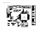
MT1389J
No EPAD
U2
LQFP128/SMD/1389L
5
6
7
8
9
10
11
12
14
15
16
17
18
19
20
21
22
23
24
25
26
27
28
29
30
31
32
33
34
36
37
38
39
40
41
42
43
44
45
46
47
48
49
52
53
54
51
57
58
55
59
60
50
62
63
61
64
65
66
67
69
70
94
90
93
92
91
89
88
84
13
35
86
79
85
83
82
81
80
78
77
76
75
74
68
73
72
4
3
2
1
128
127
126
125
124
123
118
117
116
111
110
109
108
107
106
105
104
103
102
101
100
99
98
97
96
95
112
113
122
121
120
119
115
114
56
87
71
129
AVDD12_2
AVDD33_1
XTALI
XTALO
AGND33
V20
V14
REXT / GPO5
LDO1
LDO2
AVDD33_2
DMO
FMO
TRAY_OPEN
TRAY_CLOSE
TRO
FOO
FG / GPIO2
USB_DM
USB_DP
VDD33_USB
VSS33_USB
PAD_VRT
VDD12_USB
SF_CS_
SF_DO
SF_DI
SF
_C
K
U
P1_6 /
SC
L
GPI
O
11
GPI
O
6
PR
ST
#
IR
GPI
O3 /
I
N
T
#
GPI
O
4
GPI
O13
GPI
O
9
GPI
O
8
GPI
O7 /
C
KE_
GPI
O29
GPI
O30
GPI
O31
GPI
O32
RD0
RD1
RD2
DV
DD33
RD4
RD5
RD3
RD6
RD7
D
VSS33
RD15
RD14
DQ
M0
RD13
RD12
RD11
RD10
RD8
DQM1
GPIO10
RA1
SPDIF / GPIO12
RA3
RA2
RA0
RA10
DVDD33
MDI1
U
P1_7 /
SD
A
BA1
RA4
BA0
RAS#
CAS#
DVSS12
RWE#
RA5
RA6
RA7
RA8
RA9
RD9
RA11
RCLK
RFF
RFE
RFD
RFC
RFB
RFA
RFH / O
P
INN
R
F
G /
OPI
N
P
RFIN / O
P
O
U
T / G
P
I3
6
RFIP
A
L
F / CE
NTE
R / G
P
IO
ALS /
GPI
O
A
L
/ G
P
IO
1
AD
AC
VSS1
AD
AC
VSS2
AAD
V
D
D
AKI
N
1 /
GPI
O21 /
Audio_M
u
te
AD
VC
M
/
GPI
O20
AKI
N
2 /
GPI
O19 /
Audio_M
u
te
AAD
VSS
R
B
G
DA
CV
DDB
CV
B
S
DA
CV
S
S
C
FS
VR
EF
/
GPO14
DACVDDC
GPIO33
AR
F
/
LF
E /
GPI
O
AR
S /
GPI
O
A
G
ND1
2
AVD
D
12_1
AD
AC
VD
D
2
AD
AC
VD
D
1
AVC
M
A
R
/ G
P
IO
0
DV
DD1
2
DVDD12
DVDD33
GN
D
L5
FB
C7
27pF
C5
10u/10V
L2
FB
TP3
CB14
0.1uF
+
CE9
100uF/16v
R34
0R
+
CE12
220uF/16v
TOP
HA1
HEADER 24 SMD0.5 TOP
CON0.5MM-24P-L
1
2
3
4
5
6
7
8
9
10
11
12
13
14
15
16
17
18
19
20
21
22
23
24
26
25
R7
1R
C1
1
10u/
1
0V
Q5
2N3904
2
1
3
+
CE8
47uF/16V
C4
0.1uF
Y1
27MHz
CB17
0.1uF
R36
4.7k
L9
FB
D21
ESD0603/SMD
TP
4
8
CB15
0.1uF
R24
4.7K
CB7
0.1uF
CB18
0.1uF
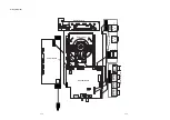
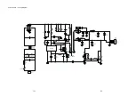
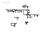
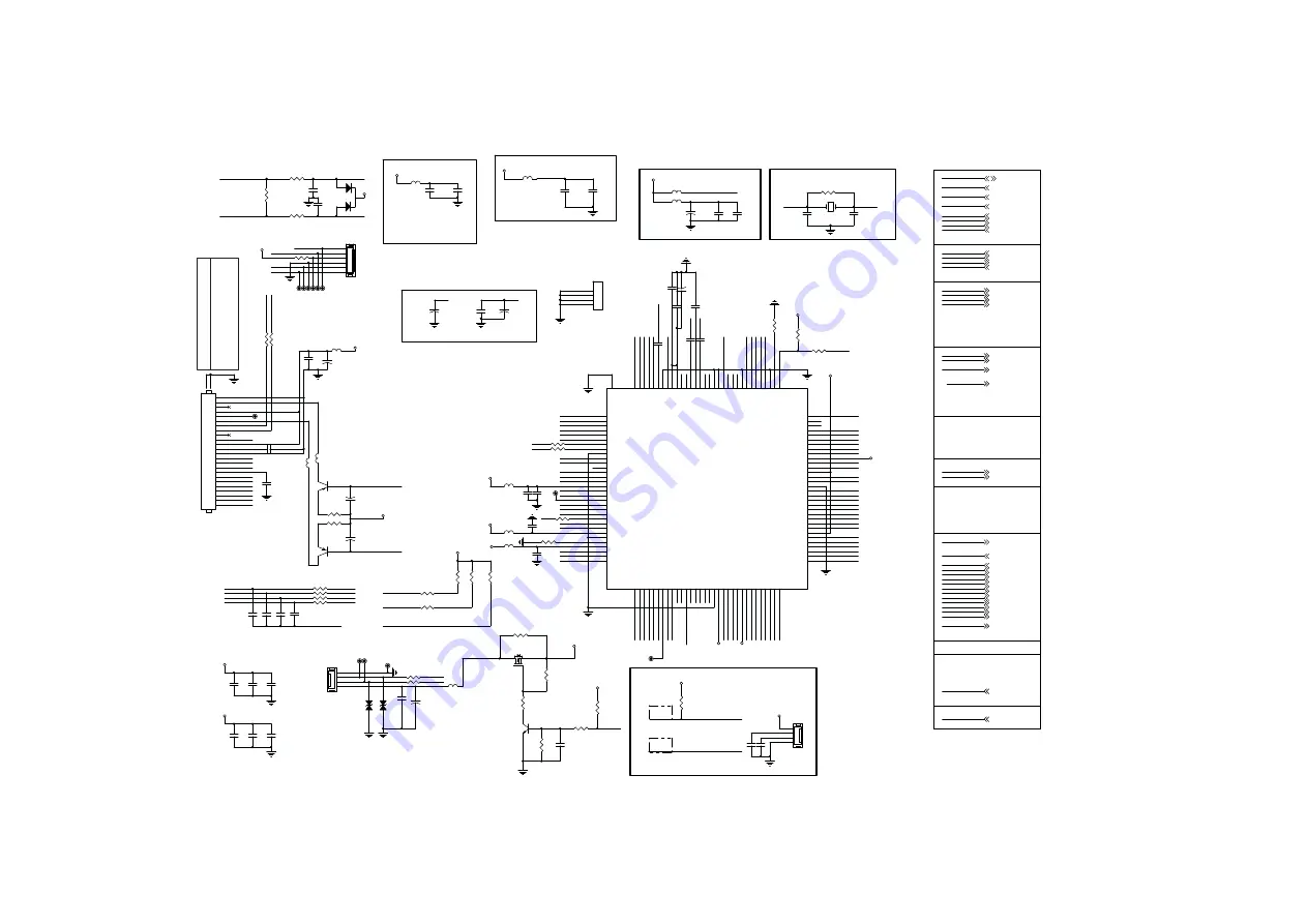
Decoder Board -- Circuit Diagram 2
12-7
12-7
Summary of Contents for MCD2010/12/93
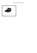
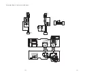
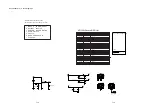
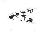
Page 26: ...8 2 Fig D4 Cabinet Disassembly Instructions ...
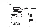
Page 33: ...Display Board Layout Diagram 12 3 12 3 ...
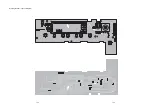
Page 35: ...Power Board Layout Diagram 12 5 12 5 ...
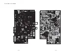
Page 42: ...Decoder Board Layout Diagram 12 12 12 12 ...
Page 44: ...Revision List Revision List Version 1 0 Initial Release 14 1 ...


