background image

LAYOUT DIAGRAM - MAIN PCB - TOP

8 - 9

8 - 9

Summary of Contents for MCD299

Page 1: ...CD playability 1 Specifications 2 Connection Controls 3 Disassembly Instructions 4 Block Wiring diagrams 5 TUNER BOARD 6 AMP BOARD 7 MAIN BOARD 8 EXPLODE DIAGRAM 11 SERVICE PARTLIST 12 DISPLAY BOARD 9 KEY1 KEY2 BOARD 10 MCD299 98 ...

Page 2: ...ICE AIDS GB WARNING All ICs and many other semi conductors are susceptible to electrostatic discharges ESD Careless handling during repair can reduce life drastically When repairing make sure that you are connected with the same potential as the mass of the set via a wrist wrap with resistance Keep components and tools also at this potential ESD CLASS 1 LASER PRODUCT GB Safety regulations require ...

Page 3: ...replace CD Drive Laser current ok N Y check Laser current CD Drive offsets ok N Y check CD Drive offsets clean the lens check playability return set Customer complaint CD related problem return set return set replace CD Drive return set replace CD Drive return set replace Signal Processor return set fast lens cleaning 1 2 3 4 5 6 7 For flap loaders access to CD drive possible cleaning method 4 is ...

Page 4: ...ted to contact the workshop directly The lens cleaning method 3 should be mentioned in the addendum sheet The final wording in national language as well as the printing is under responsibility of the Regional Service Organizations 3 FAST LENS CLEANING dry brush Use lens cleaning CD SBC AC300 9082 100 00043 Insert the lens cleaning CD press PLAY and follow the voice guide s instructions on the CD 4...

Page 5: ... with a DC Millivoltmeter directly on the connector see drawing below Pin numbering varies from drive to drive The values from diode A D should read 0 10mV Diodes E and F are less critical If one of the offsets is higher than 10mV the CD drive has to be replaced Otherwise replace the Signal Processor Sanyo DA12T3 CD Drive A A F C B E C D E VCC B VREF F D 9 10 11 12 13 14 15 16 1800 5V_HF VrefCD10 ...

Page 6: ... s V1 1 support MP3 and WMA files Number of albums folders maximum 99 Number of tracks titles maximum 999 TUNER FM wave range 87 5 108 MHz Sensitivity at 75 Ω mono 26 dB signal to noise ratio 2 8 µV stereo 46 dB signal to noise ratio 61 4 µV Tuning grid 9 10 kHz Selectivity 15 dB Total harmonic distortion 5 Frequency response 40 5000 Hz 6 dB Signal to noise ratio 58 dBA SPEAKERS Front Speakers Imp...

Page 7: ...allation Subwoofer A V cord Step 2 Antennas Connection Connect the supplied MW loop antenna and FM antenna to the respective terminals Adjust the position of the antenna for optimal reception MW Antenna Position the antenna as far as possible from a TV VCR or other radiation source FM Antenna 1 2 For better FM stereo reception connect an outdoor FM antenna to the FM ANTENNA terminal Step 1 Connect...

Page 8: ...ssive Scan feature Note If your TV does not support Progressive Scan you will not be able to view the picture Step 4 Placing the set and speakers With the supplied detachable stands and wall mounting kit you can either place the main set and speakers on desktop or mount them onto wall Desktop installation is taken for example here For how to mount the system onto wall please refer to Appendix and ...

Page 9: ...ore connecting the USB plug first slide open the protective cover on the socket By connecting a USB mass storage device including USB flash memory USB flash players or memory cards to the Hi Fi system you can enjoy the device s stored music through the powerful speakers of Hi Fi system Insert the USB device s USB plug into the socket on the set for the devices with USB cables 1 Insert one plug of ...

Page 10: ...isc USB searches fast backward forward In DISC mode to select a movement direction in the disc menu or system menu bar for clock timer to set the hour 8 3 4 In DISC mode to select a movement direction in the disc menu or system menu bar selects different slow playback modes for a VCD SVCD DVD Press and hold the button for more than three seconds 9 OK to exit or confirm the selection 0 í ë Disc ski...

Page 11: ...ove the CD Door Track then remove Left and Right CD Door 5 screws each on the upper under side Detaching the Control Panel Ass y from the Front Panel Ass y Figure 1 Figure 3 Figure 4 1 Loosen 11 screws E see Figure 4 to remove the Control Panel Ass y Figure 2 Dismantling of the Front and Rear Panel assembly B B A C D E Detach the speaker stands in the same way as you do the main unit stand To deta...

Page 12: ...ner Board and or CD Module completely unless the fault is sus pected to be in that area This will not affect the performance of the rest of the set Note The flex cables are very fragile care should be taken not to damage them during repair After repair be very sure that the flex cables are inserted properly into the flex sockets before encasing otherwise faults may occurs ...

Page 13: ... 12V 12V GND 13V ECO POWER 20V GND 20V MCU5 6V AC INPUT 120V 230V LCD 28PIN AUX IN SUB 100W L 50W R 50W LIN OUT HEADPHONE GY365 TUNER CONTROL OSC USB JACK BA5954 DRIVER DVD LOADER 1 DVD LOADER 2 DVD LOADER 3 DVD LOADER 4 BA5954 DRIVER BA5954 DRIVER BA5954 DRIVER IC 4052x 11 HT1622 RDS SAA6581T COAXIAL IC RC4558D Keystoke IR 32 768MHZ 10MHZ TDA7291x2 Open Door SUB PCB 24C01 24C02 SET BLOCK DIAGRAM ...

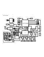
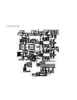
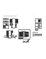
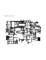
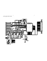
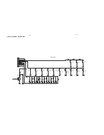
Page 14: ...WIRING DIAGRAM 5 2 5 2 ...

Page 15: ... B C D E F G 8 3V 4 0V 0 7V 0V 0 7V 0 7V 6 7V 450kHz LW only set is tuned to a strong 0 1V 1 4V 2106 E3 2107 E4 2108 G3 2109 G3 2118 H6 5 6 7 8 9 10 11 12 13 14 1 2 3 4 8 2V 8 9V 0 1V 11V 0 8V 0V 0V 0V 1 6 8V 1 2V MW HIGH A FM IF1 1 2V 0 7V 5 6 7 F G H I 1101 A2 1102 B1 1103 E2 1110 B2 1120 E14 1130 A2 1131 C1 1132 F13 2102 B2 2105 A2 0 7V mono 4 8V voltages measured while 0V 9V 5V 8 9V 1 4V 0 7V ...

Page 16: ...rame antenna has to be used 2 RC network serves for damping the IF filter while adjusting the other one 4 MW has to be aligned before LW Waverange Input frequency Input Tuned to Adjust Output Scope Voltmeter FM 87 5 108MHz 65 81 74 87 5 108MHz FM MW version 9kHz grid 531 1602kHz as low as possible ECO6 System non Cenelec stage 3 120900 TUNER BOARD ECO6 Systems non Cenelec componentside view 1101 A...

Page 17: ... HW 19 VSSP2 20 OUT2 21 BOOT2 22 VDDP2 23 VSSD 24 U502 2C413 474 2R402 5 6K 2C415 330 2C321 474 2R331 5 6K 2C322 474 2R332 5 6K L 2R602 1K 2D603 1N4148 R 2R603 1K 2D604 1N4148 L R 20V 2R321 15k 7 5 6 B 8 U302B NJM4558 2R315 68k 2R316 4 7k 2C303 10P 2C309 104 12V 2C312 823P 2C306 0 22UF 25V 2R303 82k 2R304 82k 2R309 56k 2R310 56k SW IN SW IN 2R325 82k 2R317 2 7k 2R314 2k 2C319 100P 2R324 15k 2R318 ...

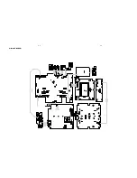
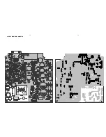
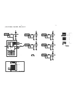
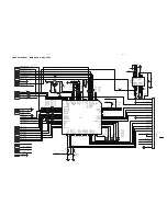
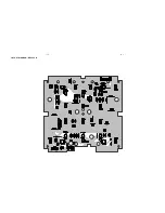
Page 18: ...LAYOUT DIAGRAM AMP PCB 7 2 7 2 ...

Page 19: ...2 HDMI Card Reader Integrated Design V2 URST URST V18 VCC 12V AVCC VCC_AUDIO DV33 5VV RFV33 GND 92_DV33 DVDD18 URST 2 7 V18 2 VCC 2 3 4 5 6 7 12V 4 5 6 AVCC 2 3 4 5 6 7 GND 2 3 4 5 6 7 VCC_AUDIO 2 3 4 5 6 7 DV33 2 3 5 5VV 2 3 4 5 6 7 RFV33 2 FB18 2 FB33 2 92_DV33 7 DVDD18 7 DV33 V18 RFV33 DV33 92_DV33 DVDD18 12V AVCC 5VV MO_VCC VCC_AUDIO VCC CE3 220uF 16V R2 10K CE1 220uF 16V CE5 10uF L1 FB CN1 CO...

Page 20: ...uF CE13 47uF C16 1000pF C41 0 1uF U13D OPEN 9 8 14 7 C13 100pF Pin Assignment v1 5 MT1389HD U1 MT1389DE H 2 250 3 4 5 1 252 253 6 7 8 9 10 11 12 13 14 15 16 17 18 19 20 21 22 23 256 28 27 30 29 32 31 43 26 25 33 34 35 36 42 41 45 39 40 46 38 37 59 75 74 72 71 70 69 68 52 91 62 63 87 86 64 65 84 83 82 81 73 93 53 54 55 56 80 57 58 67 92 85 60 61 76 78 90 79 66 77 94 95 96 97 98 99 100 101 102 103 1...

Page 21: ...SYNC 2 SPDATA 2 SPLRCK 2 SPBCK 2 SPMCLK 2 YUV7 2 DV33 DV33 SD33 DV33 FLASH_VCC FLASH_VCC DV33 VCC SD33 FLASH_VCC SD33 SD33 DV33 R56 33 R68 10K J6 Card Reader CN FFC40P 0 5 SMT 2 4 6 8 10 12 14 16 18 20 22 24 26 28 30 32 34 36 38 40 1 3 5 7 9 11 13 15 17 19 21 23 25 27 29 31 33 35 37 39 L9 J P C83 0 1uF R57 33 R60 33 R58 33 R62 33 R69 10K U6 FLASH 16M 25 24 23 22 21 20 19 18 8 10 28 47 16 29 31 33 ...

Page 22: ... RGB_SWITCH 2 12V 1 5 6 SC 5 CVBS_O 5 5VV 1 2 3 5 6 7 YUV_V 5 YUV_Y 5 YUV_U 5 YUV 1 6 2 7 5VV 12V 5VV 5VV 5VV 5VV 5VV 5VV 5VV R80 0 D6 1S1335 2 1 R81 0 C96 47pF L11 1 8uH D10 1S1335 2 1 C89 47pF R75 10 D8 1S1335 2 1 CE20 OPEN J7 SCART AUDIO 1 2 3 R74 75 1 C91 47pF C95 0 1uF R82 75 1 L15 1 8uH L10 1 8uH C97 47pF C94 47pF R70 75 1 R73 75 1 D12 1S1335 2 1 R72 75 1 D13 1S1335 2 1 C87 47pF R71 75 1 D3 ...

Page 23: ...000pF JK1 JACK 2 1 3 4 5 C98 100pF U12 OPEN 5 1 2 3 16 14 15 13 6 7 8 12 11 10 4 9 VDD BCK DATA LRCK SCK MC ML MD VCC VOUTL VOUTR ZEROL NA ZEROR ZEROA VCOM DGND AGND R118 180K R127 180K CE39 10uF 10V C123 1uF U11A NJM4558 OPA 3 2 1 8 4 C128 100pF R144 33 R94 180K R109 22K C135 0 1uF R110 22K R116 5 1K C131 27pF FB11 FB 1 2 C130 0 1uF R86 0 FB12 FB 1 2 C106 1uF Q10 2N3904 FB13 FB 1 2 C101 1000pF R1...

Page 24: ...539 104 M5V L514 100MHZ SWA SWB X0 12 X1 14 X2 15 X3 11 Y0 1 Y1 5 Y2 2 Y3 4 B 9 A 10 INH 6 VSS 8 VEE 7 VDD 16 Y COM 3 X COM 13 IC511 IC_TC4052B C540 104 M5V FB515 100MHZ SWA SWB X0 12 X1 14 X2 15 X3 11 Y0 1 Y1 5 Y2 2 Y3 4 B 9 A 10 INH 6 VSS 8 VEE 7 VDD 16 Y COM 3 X COM 13 IC512 IC_TC4052B C541 104 M5V L516 100MHZ SWA SWB X0 12 X1 14 X2 15 X3 11 Y0 1 Y1 5 Y2 2 Y3 4 B 9 A 10 INH 6 VSS 8 VEE 7 VDD 16...

Page 25: ... R414 10K C439 104 D403 1N4148 AMUTE AMUTE R459 4 7K R460 4 7K R461 4 7K C459 10U 16V C460 10U 16V Q409 BC817 Q408 BC817 R454 1K R455 1K R437 1 5K R436 1 5K C463 4 7U 16V C464 4 7U 16V 12VA 1 9 2 10 3 11 4 12 5 13 6 14 7 15 8 CN404 TO SUB L R Lin ECO CTL ECO CTL CLASSD1 MT MCU 5V Q407 8050 R453 220 C405 100U 16V C433 104 L LIN ZD402 12V C432 104 C427 333 R448 47K R447 10K C454 472 C456 0 082U C465...

Page 26: ...K R112 1K R107 1K R113 1K SWA SWB QUAL 1 RDATA 2 VREF 3 MUX 4 VDD1 5 VSS1 6 VSS3 7 CMP 8 T2 9 T1 10 VSS2 11 VDD2 12 X1 13 XO 14 NC 15 RCLK 16 IC103 SSA6581 RDS DA RDS DA C190 102 R129 10 C186 104 C191 560 R130 10 C187 104 XL103 4 332MHZ C185 22 C184 22 RCLK RCLK SWA SWB R115 1K R117 1K R116 1K R114 1K GND MCU 5V PO CTL AMUTE TU CTL DV CT 7 DA 7 CL ECO R101 1K R102 1K R126 10K R118 22 R122 330 R121...

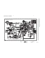
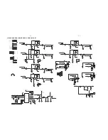
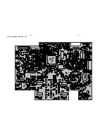
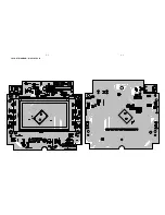
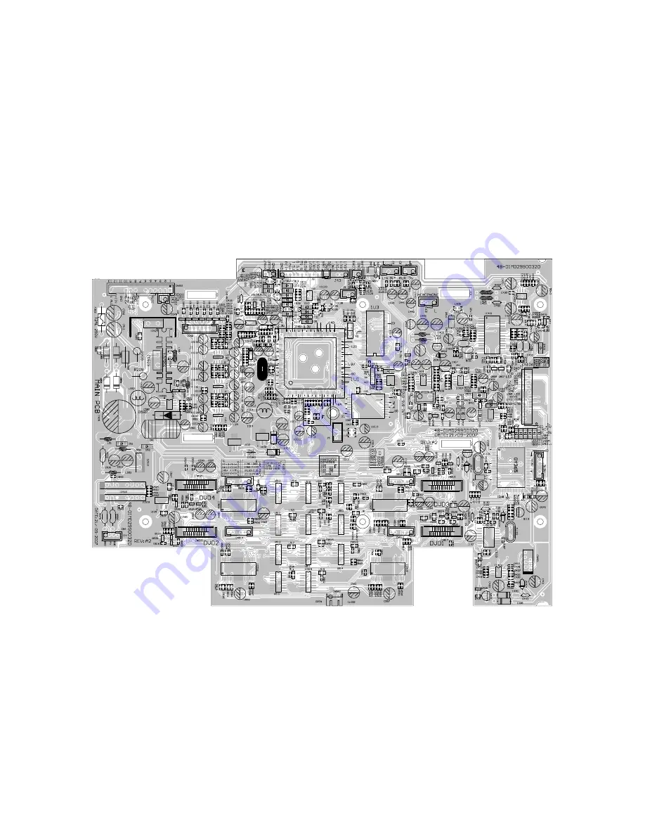
Page 27: ...LAYOUT DIAGRAM MAIN PCB TOP 8 9 8 9 ...

Page 28: ...LAYOUT DIAGRAM MAIN PCB BOTTOM 8 10 8 10 ...

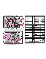
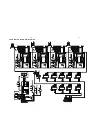
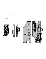
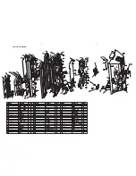
Page 29: ...LAYOUT DIAGRAM VIDEO PCB USB PCB VGA PCB USB PCB VGA PCB VIDEO PCB 8 11 8 11 ...

Page 30: ...09 LCD10 LCD11 LCD12 LCD13 LCD14 LCD15 LCD16 LCD17 LCD18 LCD19 LCD20 LCD21 LCD22 LCD23 LCD24 LCD25 LCD26 LCD27 LCD28 LCD01 LCD02 LCD03 LCD04 LCD05 LCD06 LCD07 LCD08 LCD09 LCD10 LCD11 LCD12 LCD13 LCD14 LCD15 LCD16 LCD17 LCD18 LCD19 LCD20 LCD21 LCD22 LCD23 LCD24 LCD25 LCD26 LCD27 LCD28 MCU 5V LED VCC Q215 8050 Q218 8050 LED401 wite R241 470 R242 470 R239 470 R243 470 R240 470 R244 470 R246 470 R245 ...

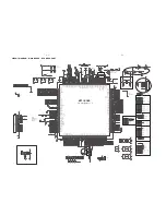
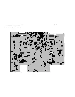
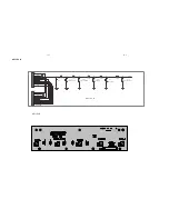
Page 31: ...LAYOUT DIAGRAM DISPLAY PCB 9 2 9 2 ...

Page 32: ... TIMER R385 470 1 TA306 SOURCE R387 560 1 TA307 PROGRAM R390 680 1 TA310 R OPEN CLOSE KEY011 KEY011 KEY1 LED VCC LED GND USB LED KEY01 KEY1 LED VCC LED GND USB LED 1 2 3 4 5 6 7 8 9 10 CON207 CN10 20 USBP USBM GND USB GND GND 1 2 3 4 5 6 7 8 9 10 CN304 CN10 20 USBP USBM GND USB GND KEY1 PCB ...

Page 33: ...104 LED304 BLUE LED303 BLUE LED302 BLUE LD301 BLUE R367 150 1 TA303 VOL C376 102 R382 220 1 TA302 VOL R384 330 1 TA305 ALBUN R386 470 1 TA308 PLAY PAUSE R388 560 1 TA309 ALBUM R389 680 1 TA313 TITLE R392 820 1 TA12 STOP R394 1 2K 1 TA316 TITLE R396 2 2K 1 TA317 DVD4 PRESE TA311 DVD1 R393 1 2K 1 TA315 DVD2 R395 2 2K 1 TA314 DVD3 R391 820 1 KEY011 KEY1 LED VCC LED GND USB LED 1 2 3 4 5 6 7 8 9 10 CO...

Page 34: ...10 3 10 3 LAYOUT DIAGRAM KEY2 PCB ...

Page 35: ...65 000 40384 9965 000 40383 9965 100 01577 9965 000 40386 9965 000 40385 9965 100 09474 9965 100 09435 9965 100 09436 9965 100 09432 9965 100 09434 9965 000 40387 9940 000 02818 9940 000 02815 9965 100 09475 9965 100 01578 9965 100 09433 9965 100 01579 9965 100 01581 9965 100 01584 9965 100 09439 9965 100 01573 9965 100 09473 9965 100 01580 11 1 11 1 EXPLODE DIAGRAM ...

Page 36: ...21 9965 000 40384 CD DOOR RIGHT 68 9965 100 01580 DISPLACE COVER 25 9965 000 40385 ROLLER BOTTOM GEAR 24 9965 000 40386 ROLLER TOP GEAR 31 9965 000 40387 DRIVER PULLEY 10 9965 000 40388 STAND KEY 16 9965 000 40389 SOURCE KEY 65 9965 100 01581 USB LIGHT GUIDE LENS 4 9965 100 01582 CONTROL KEY LIGHT GUIDE LENS 14 9965 100 01583 LCD LIGHT GUIDE 20 9965 000 40392 CD DOOR LENS L 19 9965 000 40393 CD DO...

Page 37: ...965 100 09448 CRYSTAL27MHzHC49 US30PF 20PPM 2CN301 9965 100 09458 3 12P SHIELD WIRE L 180 120mm CN106 9965 100 09451 F F C WAFER 1 25mm 21P 90C CN401 9965 100 06596 F F C WAFER 1 25mm 8P 180C CN402 9965 100 09454 3P 4P SHIELD WIRE L 110mm CN403 9965 100 09457 4P SHIELD WIRE L 170mm D509 9965 000 42437 CH DIODE SS14 SMA DO 214AC D511 9965 000 42437 CH DIODE SS14 SMA DO 214AC D580 9965 100 09446 DIO...

Page 38: ...SK3018 Q524 9965 100 09477 SMD TRANSISTORS 2SK3018 Q525 9965 100 09477 SMD TRANSISTORS 2SK3018 Q526 9965 100 09477 SMD TRANSISTORS 2SK3018 Q527 9940 000 04338 SMD TRANSISTORS PMBT3904 Q528 9940 000 04338 SMD TRANSISTORS PMBT3904 Q529 9940 000 04338 SMD TRANSISTORS PMBT3904 Q53 9940 000 04338 SMD TRANSISTORS PMBT3904 Q530 9940 000 04338 SMD TRANSISTORS PMBT3904 Q580 9940 000 04338 SMD TRANSISTORS P...

Page 39: ...0 42438 LED LAMP 2x5x7mm WHITE LED402 9965 000 42438 LED LAMP 2x5x7mm WHITE LED403 9965 000 42438 LED LAMP 2x5x7mm WHITE LED404 9965 000 42438 LED LAMP 2x5x7mm WHITE LED405 9965 000 42438 LED LAMP 2x5x7mm WHITE LED406 9965 000 42438 LED LAMP 2x5x7mm WHITE LED407 9965 000 42438 LED LAMP 2x5x7mm WHITE LED408 9965 000 42438 LED LAMP 2x5x7mm WHITE LED421 9940 000 01965 LED LAMP 3MM RED Q22 9940 000 04...

Page 40: ...A311 9965 000 42445 TACT SWITCH 6x6mm 7mm TA312 9965 000 42445 TACT SWITCH 6x6mm 7mm TA313 9965 000 42445 TACT SWITCH 6x6mm 7mm TA314 9965 000 42445 TACT SWITCH 6x6mm 7mm TA315 9965 000 42445 TACT SWITCH 6x6mm 7mm TA316 9965 000 42445 TACT SWITCH 6x6mm 7mm TA317 9965 000 42445 TACT SWITCH 6x6mm 7mm ELECTRICAL PARTS VIDEO PCB CN681 9965 100 09465 RCAJACK 2P WH RD RJ2P361093 44 J38 9965 100 09463 PH...

Reviews: