background image

5-6

5-6

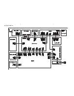
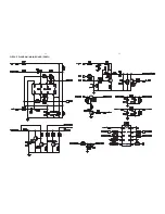
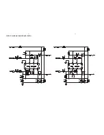
CIRCUIT DIAGRAM - MAIN BOARD (PART4)

Summary of Contents for MCD355

Page 1: ...on of Philips Published by SL 0920 Service Audio Printed in The Netherlands Subject to modification DVD Micro Theater Version 1 0 CLASS 1 LASER PRODUCT 3141 785 34150 TABLE OF CONTENTS Page PCBs Location 1 2 Specifications 1 3 Measurement Setup 1 4 Service Aids Safety Instruction etc 1 5 to 1 7 Software Version Checking 2 Set Block Diagram 3 Set Wiring Diagram 4 Main Headphone AUX Board 5 VFD Boar...

Page 2: ...1 2 PCBS LOCATION ...

Page 3: ... rate data rate 32 320 Kbps and variable bit rate WMA v9 or earlier Directory nesting up to a maximum of 8 levels Number of albums folders maximum 99 Number of tracks titles maximum 999 ID3 tag v2 0 or later File name in Unicode UTF8 maximum length 128 bytes Unsupported formats Empty albums an empty album is an album that does not contain MP3 WMA files and is not be shown in the display Unsupporte...

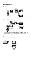
Page 4: ...7122 707 89001 Tuner AM MW LW To avoid atmospheric interference all AM measurements have to be carried out in a Faraday s cage Use a bandpass filter or at least a high pass filter with 250Hz to eliminate hum 50Hz 100Hz RF Generator e g PM5326 Ri 50 Bandpass 250Hz 15kHz e g 7122 707 48001 LF Voltmeter e g PM2534 DUT RF Generator e g PM5326 S N and distortion meter e g Sound Technology ST1700B Use a...

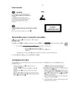
Page 5: ...ng make sure that you are connected with the same potential as the mass of the set via a wrist wrap with resistance Keep components and tools also at this potential ESD CLASS 1 LASER PRODUCT GB Safety regulations require that the set be restored to its original condition and that parts which are identical with those specified be used Safety components are marked by the symbol Lead free ...

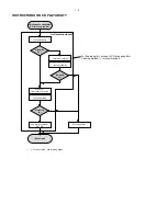
Page 6: ...T OK check playability N Y playability ok check playability check playability return set Customer complaint CD related problem fast lens cleaning 1 2 3 For flap loaders access to CD drive possible cleaning method 4 is recommended INSTRUCTIONS ON CD PLAYABILITY 1 6 Exchange CDM 1 4 For description see following pages ...

Page 7: ...viously caused by a scratched dirty or copy protected CD In case problems remain the customer is requested to contact the workshop directly The lens cleaning method 3 should be mentioned in the addendum sheet The final wording in national language as well as the printing is under responsibility of the Regional Service Organizations 4 LIQUID LENS CLEANING Because the material of the lens is synthet...

Page 8: ...3 1 3 1 SET BLOCK DIAGRAM ...

Page 9: ...SET WIRING DIAGRAM 4 1 4 1 ...

Page 10: ...MAIN HP JACK AUX JACK BOARD TABLE OF CONTENTS Main PCB Layout Top View 5 2 Main PCB Circuit Diagram 5 3 to 5 10 Headphone Jack PCB 5 11 AUX Jack PCB 5 12 5 1 5 1 ...

Page 11: ...5 2 5 2 PCB LAYOUT MAIN BOARD TOP VIEW ...

Page 12: ...5 3 5 3 CIRCUIT DIAGRAM MAIN BOARD PART1 ...

Page 13: ...5 4 5 4 CIRCUIT DIAGRAM MAIN BOARD PART2 ...

Page 14: ...5 5 5 5 CIRCUIT DIAGRAM MAIN BOARD PART3 ...

Page 15: ...5 6 5 6 CIRCUIT DIAGRAM MAIN BOARD PART4 ...

Page 16: ...5 7 5 7 CIRCUIT DIAGRAM MAIN BOARD PART5 ...

Page 17: ...5 8 5 8 CIRCUIT DIAGRAM MAIN BOARD PART6 ...

Page 18: ...5 9 5 9 CIRCUIT DIAGRAM MAIN BOARD PART7 ...

Page 19: ...5 10 5 10 CIRCUIT DIAGRAM MAIN BOARD PART8 ...

Page 20: ...5 11 5 11 PCB LAYOUT HEADPHONE JACK BOARD CIRCUIT DIAGRAM HEADPHONE JACK BOARD ...

Page 21: ...5 12 5 12 PCB LAYOUT AUX JACK BOARD CIRCUIT DIAGRAM AUX JACK BOARD ...

Page 22: ...OARD TOUCH KEY BOARD TABLE OF CONTENTS VFD PCB Layout Top View 6 2 VFD PCB Layout Bottom View 6 3 VFD PCB Circuit Diagram 6 4 to 6 6 Touch Key PCB Layout Diagram 6 7 Touch Key PCB Circuit Diagram 6 8 6 1 6 1 ...

Page 23: ...6 2 6 2 PCB LAYOUT VFD BOARD TOP VIEW ...

Page 24: ...PCB LAYOUT DISPLAY PANEL BOARD BOTTOM VIEW 6 3 6 3 ...

Page 25: ...6 4 6 4 CIRCUIT DIAGRAM VFD BOARD PART1 ...

Page 26: ...6 5 6 5 CIRCUIT DIAGRAM VFD BOARD PART2 ...

Page 27: ...6 6 6 6 CIRCUIT DIAGRAM VFD BOARD PART3 ...

Page 28: ...6 7 6 7 PCB LAYOUT TOUCH KEY BOARD ...

Page 29: ...6 8 6 8 CIRCUIT DIAGRAM TOUCH KEY BOARD ...

Page 30: ...SERVO BOARD 7 1 7 1 The servo board is not intended to repair on components level The dia grams only for reference The whole board can be ordered with 12nc 996510025795 ...

Page 31: ...7 2 7 2 PCB LAYOUT SERVO BOARD TOP VIEW ...

Page 32: ...7 3 7 3 PCB LAYOUT SERVO BOARD BOTTOM VIEW ...

Page 33: ...7 4 7 4 CIRCUIT DIAGRAM SERVO BOARD PART1 ...

Page 34: ...7 5 7 5 CIRCUIT DIAGRAM SERVO BOARD PART2 ...

Page 35: ...7 6 7 6 CIRCUIT DIAGRAM SERVO BOARD PART3 ...

Page 36: ...7 7 7 7 CIRCUIT DIAGRAM SERVO BOARD PART4 ...

Page 37: ...7 8 7 8 CIRCUIT DIAGRAM SERVO BOARD PART5 ...

Page 38: ...7 9 7 9 CIRCUIT DIAGRAM SERVO BOARD PART6 ...

Page 39: ...7 10 7 10 CIRCUIT DIAGRAM SERVO BOARD PART7 ...

Page 40: ...7 11 7 11 CIRCUIT DIAGRAM SERVO BOARD PART8 ...

Page 41: ...7 12 7 12 CIRCUIT DIAGRAM SERVO BOARD PART9 ...

Page 42: ...USB POWER KEY BOARD 8 1 8 1 ...

Page 43: ...8 2 8 2 PCB LAYOUT USB JACK BOARD CIRCUIT DIAGRAM USB JACK BOARD ...

Page 44: ...PCB LAYOUT POWER KEY BOARD 8 3 8 3 CIRCUIT DIAGRAM POWER KEY BOARD ...

Page 45: ...3 7 B 6 D A G 4 2 14 13 C 5 10 11 8 1 9 8 1 8 1 SET MECHANICAL EXPLODED VIEW ...

Page 46: ...64M M12L64164A 7TG C 996510025795 SERVO PCB IC605 996510005002 IC D2761 SILICORE IC306 996510010762 IC AM5888S HSOP28 D 996510025821 MCD355 VFD PCB IC606 996510001055 IC BA4558 SOP8 IC602 996510001055 IC BA4558 SOP8 D 996510025821 MCD355 VFD PCB IC606 996510001055 IC BA4558 SOP8 IC602 996510001055 IC BA4558 SOP8 G 996510025814 SWITCHING POWER SUPPLY MODULE IC607 996510001055 IC BA4558 SOP8 Q103 99...

Page 47: ...025037 VFD FOR MCM355 ZD402 996510012835 ZENER DIODE 5V6 1 2W TC5V6 ZD402 996510012835 ZENER DIODE 5V6 1 2W TC5V6 HEADPHONE JACK PCB ASSY HEADPHONE JACK PCB ASSY JA502 994000001456 STEREO HEADPHONE JACK AUX JACK PCB ASSY JA602 996510001073 EARPHONE CKX3 5 19S 3PIN JA602 996510001073 EARPHONE CKX3 5 19S 3PIN Note Only these parts mentioned in the list are y p normal service parts 7 3 ...

Reviews: