background image

CD_TRIN

RX

VREF_16

XSLEGP

TPI

FOCUS+

XSPINDLE

SPIN+

FOCUS

SL-

F_DO

LIMIT

MCPUH

F_CLK

TNI

FOCUS-

MBPUH

SSDA

VREF_16

MDI

USB5V

MCPUH

SBLPFO

LIMIT

FOCUS-

XSPINDLE

VREF_16

TRACK

CD_TRIN

CD_MUTE

SLEGP

F_CS

TELPFO

FOCUS+

LD

MUTE34

SPIN-

TX

VREF_16

SL+

XTRACK

TRACK+

HAVC

TX

XFOCUS

TPI

RX

MAPUH

TNI

F_DI

MDI

SPIN+

HAVC

TRACK-

SPINDLE

SL+

SPIN-

MBPUH

CD_MUTE

F_CS

XFOCUS

TRACK+

F_DI

HOLD#

XSLEGP

SPIN+

MAPUH

SPIN-

F_DO

MDPUH

LIMIT

SSCL

R32

10K

R30

10K

R31

330R

LDO

FELPFO

MDPUH

VREF_16

SL-

F_CLK

WP

VREF_16

MUTE34

XTRACK

GND

LD

M+

GND

M-

OPEN_SW

CLOSE_SW

D+

CD_R

RESETJ

CD_L1

CD_R1

LRCK

+3.3V

MCLK

SDATA

SCLK

CDR

CD_L

SCLK

MCLK

SDATA

LRCK

CDL

CD_L

CD_R

CD_L1

CD_R1

SPIN+
TRACK-

SPIN-

CD_5V

SSCL

SSDA

CD_MUTE

CD_TRIN

M33V

V

18_CO

R

E

SEV_3V3

3V3SD_IC

3V3SD

AUD_3V3

M33V

M33V_LDO

M33V_CKG

M33V_PAD

+5.6V

M33V_LDO

3V3SD

M33V_PAD

+5.6V1

RF_1V8

SEV_3V3

M33V

3V3SD

V18_CORE

3V3SD

V18

3V3SD

M33V

+5.6V1

3V3SD

3V3SD

SEV_3V3

3V3SD

3V3SD_IC

V18

M

33V

_P

A

D

SEV_3V3

V18_CORE

M33V_CKG

RF_1V8

+5.6V

3V3SD

AUD_3V3

AUD_3V3

+5.6V1

M3

3

V

_

P

AD

+5.6V

+5V

+5V

+3.3V

+5.6V

+5.6V

CDR

2

CDL

2

Ferrite Bead 500mA

R2

0R

R6

10K/NC

C20

104

C44

1uF/50V

1

2

3

4

CON4

CON2.0-4

R9

560K

/0

R15

10K

L11 DCR33

R55
100K

L6 DCR33

C18

473

TX

EC19

10uF/16V

1

2

3

4

5

CON2

CON2.0-5

C12

104

TP22

C38

104

Y1
16.9344MHz

EC6

10uF/10V

R26

4

.7K

R26

4

.7K

TP12

TP16

R18 3.3K

C41

104

EC9

470uF/10V

EC18

100uF/16V

TP9

EC11

10uF/16V

R60

22R

L10 DCR33

C40

104

R10
15R

C53

104

R1 51k

R63

10K

R49 27K

R72

33R

C36

104

VC

1

VCC

2

E

3

D

4

A

5

B

6

C

7

F

8

GND

9

LD

10

VR

11

MD

12

F+

13

T-

14

T+

15

F-

16

SF-P200Z(FPC)

CN1

R24

100k

L5

DCR33

TP15

SPIN+

1

SPIN-

2

SLED+

3

SLED-

4

LIMIT1

5

LIMIT2

6

CON1

CON2.0-6

C17

104

R23

0R

R58
2R2

C24

103

TP10

1
2
3
4
5

J2

CON5

C30

102

R19

0R

2

1

3

Q3

8550,DIP

C32

104

R17 15K

1

2

D2

1N4148

R62

22R

L7 DCR33

TE

L9 DCR33

2

2

3

3

4

4

5

5

9

9

8

8

7

7

6

6

1

1

H1

HOLE/GND

C133 474

EC10

1000uF/10V

EC4

10uF/16V

R29

33K

R57

220R

R41 NC/0R

L3 DCR33

R66
10K

R28

4

.7K

R28

4

.7K

R56
100K

C25 104

C3

104

C50

2200P

C22

104

C10

105

C14

105

C6

104

C52

2.2uF

EC2

1000uF/10V

R3 2.2R

R16 20K

R5

1K

R11
4.7K

R47 10K

EC16

10uF/16V

R44 1.5K

R13
47K

F1

SMD0805P100TF 1A 6V

1
2

J3

CON3

TP11

2

1

3

Q1

8550,DIP

EC12

220uF/16V

TP21

EC8

10uF/10V

1

2

L13 DCR33

A

A

A

EC5

47uF/16V

R51

4.7K(NC)

R12

1K

C28
0.1UF/NC

C28
0.1UF/NC

EC15

220uF/10V

VI

NFC

1

TR

B_

1

2

RE

GO2

3

VI

NSL

+

4

RE

GO1

5

FW

D

6

REV

7

VCC1

8

VO

TR-

9

VO

TR+

10

VO

SL

+

11

VO

SL

-

12

VO

FC-

13

VO

FC+

14

VO

TK+

15

VO

TK-

16

V

OLD+

17

VO

L

D

-

18

VCC2

19

OP

IN

20

VCTL

21

GND

22

VINL

D

23

OP

OUT

24

TR

B_

2

25

VI

NTK

26

BI

AS

27

MU

T

E

28

GND

29

GND

30

U2

AM5766FM

TP18

R20
12K

C2

104

C143

474

R14
10R/0.5W

R37

33R

R35
15k

R61

22R

R48 1.5K

TP7

MK2

MK2

R8

82K

/39K

R65

10K

2

1

3

Q2

2N3904

D3
ESD

C27 30pF

EC17

10uF/16V

C33

104

1

2

D4

1N5819

TP4

C47

0.1uF

2

2

3

3

4

4

5

5

9

9

8

8

7

7

6

6

1

1

H2

HOLE/GND

C21 104

R4 3.9K

R25

330R

R25

330R

L4 DCR33

R38

33R

C9 104

C11

104

D5
NC

R53

10K

R67
10K

C42

104

C19

104

C23 30pF

TP5

C15
104

EC14

10uF/16V

D6
NC

RX

R45 22K

1

2

D7

IN4001

C35

104

D8
3.3V/SMD

2

2

3

3

4

4

5

5

9

9

8

8

7

7

6

6

1

1

H4

HOLE/GND

R34
15k

TP6

CS#

1

DO

2

WP#

3

GND

4

DI

5

CLK

6

HOLD#

7

VCC

8

U3

SFLASH EON25P20(1M bit)

C1

104

TP19

C43

104

+

CE2
22UF/6.3V/4*7

+

R27

33K

C45

2.2uF

FE

C51

2200P

1

2

D1
1N4148

C7

104

VL

1

SDIN

2

MCLK

3

LRCK

4

SCLK/DEM

5

GND

6

FILT+

7

AOUTA

8

AOUTB

9

GND

10

VA

11

FLYP

12

FLYN

13

-VFILT

14

CE4354

U4

CS4354

C49

2.2uF

C26
0.1UF/NC

C26
0.1UF/NC

TP8

SB

TP17

R59

22R

L8 DCR33

C4

104

EC13

10uF/16V

MK1

MK1

1

2

L1 DCR33

C13

104

R54

4.7K(NC)

R64

10K

TP20

1

2

3

4

CON3

CON2.0-4

EC7

10uF/10V

R42 10K

L12 DCR33

R73

33

C31 104

C48

2.2uF

C29

102

C5

103

C34

104

EC1

10uF/16V

C16 104

R21 0R

C8

474

R7
4.7K

XGPIOD7/SPDIF

71

XGPIOD1/I2CM_DAT(B)

65

XPAD_BOCAPR

35

VTP

20

XTALI

26

XPAD_

SFG

N

51

LDO

1

XAVSS33_LDO

22

XPAD_

XVREF

49

XGPIOH1/DATA4(B)

93

FM

IN

L

42

XGPIOE4/SDD0(B)

76

XGPIOH7/LCDRDJ(O)

100

XG

PI

O

C

0

/SFCSB

60

XPAD_BICAFL

31

MB

5

XGPIOD4/I2S_DO

68

XGPIOG3/USI_DI

87

XG

PI

O

C

2

/URTX

62

XGPIOH6/LCDCSJ(O)

98

XPAD_

V1

5

R

48

XPAD_

M

IC

IN

41

XGPIOH2/DATA5(B)

94

XGPIOH3/DATA6(B)

95

XPAD_

V1

5

L

46

XGPIOE2/DOCD_CLK(O)

74

MPXOUT2

14

XDP

53

COSP

16

XGPIOI0/LCDWRJ(O)

101

XGPIOF2/SD_MS_PWR

82

XGPIOF3/SD_MS_DET

83

XPAD_LINEOUTR

36

TP2

3

XGPIOE1/DOCD_DATI(I)

73

VTB

19

XAVDD33_LDO

23

XGPIOE3/SD_MS_WP

75

XAVDD33_2

8

TELP

12

XGPIOH4/DATA7(B)

96

XGPIOD6/I2S_WCLK

70

VDD_

CORE

54

MC

4

XGPIOG5/DATA0(B)

89

XPAD_

V0

8

R

47

FM

IN

R

39

XAVDD18_LDO

24

XGPIOG2/USI_DO

86

XPAD_

M

IC

BI

AS

44

XGPIOE0/DOCD_DATO(O)

72

XGPIOD3/I2S_REFCLK

67

V12

10

XAVDD33_3

18

XPAD_LINEOUTL

33

MD

6

MPXOUT1

13

XAVSS33_3

21

XPAD_

V0

8

L

45

XGPIOI1/PWM0_0(O)

102

XG

PI

O

B7

/SFDI

59

XPAD_

SFG

P

50

XGPIOF0/SDCMD(B)/MSBS(O)

80

XGPIOH0/DATA3(B)

92

XAVDD33_CKG

25

XGPIOF1/SD/MS_CLK(O)

81

VDD_

PAD

57

XPAD_

L

INEI

NR

40

XGPIOD2/I2S_SCLK

66

XGPIOG4/USI_CLK

88

XGPIOC3/URRX

63

XAVSS33_2

11

X

GP

IOD0/I2CM

_CLK

(O)

64

GND_

CORE

55

XDM

52

XGPIOH5/LCDA0(O)

97

XAVSS33_CKG

28

XPAD_

L

INEI

NL

43

XGPIOE7/SDD3(B)

79

XG

PI

O

B6

/SFDO

58

XPRSTB

99

XGPIOG6/DATA1(B)

90

HAVC

9

COSN

17

MA

7

TP1

2

GND_PAD

56

XGPIOE5/SDD1(B)

77

XGPIOD5/I2S_DI

69

XPAD_BOCAPL

32

XG

PI

O

C

1

/SFSCK

61

XTALO

27

MPXOUT3

15

XGPIOG7/DATA2(B)

91

XGPIOE6/SDD2(B)

78

XPAD_BICAPR

34

X

G

P

IOI2/IRC

103

XG

PI

O

I3

104

XG

PI

O

I4

105

XG

PI

O

I5

106

XG

PI

O

I6

107

XG

PI

O

I7

108

XG

PI

O

J

0

109

XG

PI

O

J

1

110

XG

PI

O

J

2

111

GND_

CORE

114

VDD_

CORE

115

XAVDD_

D33

116

BTN_

ADI

N

1

117

BTN_

ADI

N

2

118

BTN_

ADI

N

3

119

VREF1

6

120

FM

O

121

XAVD3

3

_

1

122

DM

O

123

XAVSS3

3

_

1

124

GP

WM

125

FO

O

126

TR

O

127

MD

I

128

XAVDD18_1

29

XAVSS18_1

30

XAVSS33_AUD

37

XAVDD33_AUD

38

GND_PAD

84

VDD_PAD

85

GND_PAD

112

VDD_

PAD

113

ALi  M5673

U1

ALi  M5673

U1

1

2

L2 3.3Ω

C46

104

R22

43k

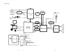
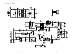
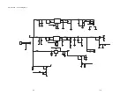
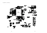
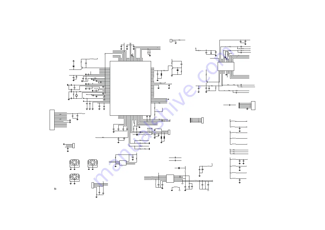
Decoder Board -- Circuit Diagram

12-8

12-8

Summary of Contents for MCM1050/12/93

Page 1: ... Important Safety Precautions 3 1 to 3 2 4 Safety Check After Servicing 4 1 6 Standard Notes For Servicing Lead Free Requirements Handling Flat Pack IC 6 1 to 6 4 5 Safety Information General Notes Lead Free 7 Direction of Use 7 1 to 7 2 8 Cabinet Disassembly Instructions 8 1 to 8 2 12 Display Board 9 Troubleshooting 9 1 to 9 2 10 Block Diagram 10 1 11 Wiring Diagram 11 1 13 Power Board 14 AMP Boa...

Page 2: ... Lever Repair Used 55 55 58 58 61 61 79 79 93 93 94 94 96 96 98 98 37 37 12 10 C C C C M M M M 12 10 05 05 Feature diffrence RDS AMP Board Decoder Board Power Board DTS VOLTAGE SELECTOR ECO STANDBY DARK Type Versions MCM1050 Technical Specification and Connection Facilities 1 1 Display Board Decoder Board Display Board Power Board AMP Board ...

Page 3: ...Amplifier ST class D TDA7491HV 7 Rated output power 10 THD table 2 Set Type Number Stroke Versions Power ROP Power Volume max Remark MCM1050 All version 2x5W 2x12W 2 1 2 Styling Forms and Functions MCM1050 appearances are defined in their respective MUS MUS is the leading document where product appearance is applicable Features Products MCM1050 Stroke versions l l A Design Refer to MUS 3 for detai...

Page 4: ...tbc Control keys on the set are 1 Standby On 2 Eject 3 Play Pause 4 Next 5 Pre 6 FF 7 FB 8 Source Disc USB Dock FM Aux MP3 9 Stop 10 Volume Knob There is local display LCD reuse Standby LED colour Red in Standby mode 2 1 5 ACCESSORIES tbc Model MCM1050 Stroke Version All Version n o i g Power Cord e R Audio cable 3 5mm audio 0 5M Remote Control 31keys Quickly guide 1 IFU 1 Technical Specification ...

Page 5: ...C Requirements Where applicable For 12 EU 05 UK 51 Russia EN55013 2001 EN55020 2002 For 37 US Canada FCC15 For 55 LATAM 78 Brazil CISPR13 For 98 AP 69 Singapore 75 Australia CISPR13 For 61 Korea CISPR13 20 For 93 China GB 13837 CISPR13 For 96 Taiwan CNS 13439 CISPR13 2 5 ESD Requirements The product shall withstand electro static discharges on all user accessible parts of the product Reference IEC...

Page 6: ...class class 2 according to BLC A MA PQR handbook V2 1 2006 10 02 Lifetime 7 years Tested According to General Test Instruction UAN D 1591 Measured According to UAN_L 1059 unless otherwise stated Technical Specification and Connection Facilities 1 5 3 Technical Specifications 3 1 Power Supply 3 1 1 Type and versions Build inSMPS will be used for all models and stroke versions All using built in Pow...

Page 7: ...eliability evaluation Requirements Apparatus should fulfil the leakage current requirements of IEC60065 point 9 1 1 UAN D1631 Defects or permanent deviations are not allowed 3 1 3 Mains Drop out Immunity The product shall withstand mains failures of Variation 0 100 dip at T event 50 mSec Performance criterion B Variation 40 60 dip at T event 100 mSec Performance criterion B Variation 0 100 dip at ...

Page 8: ... o r C Amplification Reserve 3dB 2dB Audio Inputputs Audio Input Sensitivity 3dB rated output power at 1kHz Audio Output 1 Tuner FM 67 5kHz Modulation Limit 6dB Line Out Left Right NA 2 W m 5 1 e n o h p d a e H 1 k c a r T 1 c s i D o i d u A k c a r t B d 3 3 P M D C dB RL 16Ω S H 0 2 e v a w e n i s z H K 1 B d 3 B S U MP3_link front 500mV 1000mV Rin 22kΩ Output Power 1 At THD 10 1kHz sinewave ...

Page 9: ... 4 0 e s r e v e R n o i t a c i f i l p m A 3 2 z H k 5 7 v e D q r F V m 1 F R n o i t r o t s i D Overall Frequency Response 63Hz 12 5KHz 3 dB Channel separation 400 1000 5000 Hz RF input 68 dBf 26 30 20 20 26 18 dB Frequency MHz Noise Limited Sensitivity 26 dB Image Rejection IF Rejection Large Signal Handling Selectivity S9 300 kHz 2 2 0 0 0 1 4 6 0 3 8 1 m o N M F 1 8 1 0 0 5 5 4 5 2 2 2 m i...

Page 10: ...the pickup lens when the diode is turned on Do not look directly at the laser beam CAUTION Use of controls and adjustments or doing procedures other than those specified herein may result in hazardous radiation exposure Location Inside Top of Blu Ray mechanism Do not look directly at the laser beam coming from the pickup or allow it to strike against your skin Drive Mechanism Assembly Laser Beam R...

Page 11: ... Important Important Safety Precautions Read and understand all instructions before you use your home theater If damage is caused by failure to follow instructions the warranty does not apply Safety Riskof electricshock or fire Never expose the product and accessories to rain or water Never place liquid containers such as vases near the product If liquids are spilt on or into the product disconnec...

Page 12: ...ic products Please act according to your local rules and do not dispose of your old products with your normal household waste Correct disposal of your old product helps to prevent potential negative consequences for the environment and human health Your product contains batteries covered by the European Directive 2006 66 EC which cannot be disposed with normal household waste Please inform yoursel...

Page 13: ... and externally exposed accessible parts RF terminals antenna terminals video and audio input and output terminals microphone jacks earphone jacks etc is lower than or equal to the specified value in the table below Measuring Method Power ON Insert load Z between B earth ground power cord plug prongs and exposed accessible parts Use an AC voltmeter to measure across the terminals of load Z See Fig...

Page 14: ...e sure that during repair you are at the same potential as the mass of the set by a wristband with resistance Keep components and tools at this same potential Available ESD protection equipment Complete kit ESD3 small tablemat wristband 4822 310 10671 Wristband tester 4822 344 13999 Be careful during measurements in the live voltage section The primary side of the power supply including the heatsi...

Page 15: ...older paste is required please contact the manufacturer of your solder equipment In general use of solder paste within workshops should be avoided because paste is not easy to store and to handle Use only adequate solder tools applicable for lead free solder alloy The solder tool must be able To reach at least a solder temperature of 400 C To stabilize the adjusted temperature at the solder tip To...

Page 16: ... this and more technical information within the magazine chapter workshop news For additional questions please contact your local repair helpdesk How to Remove Install Flat Pack IC 1 Removal With Hot Air Flat Pack IC Desoldering Machine 1 Prepare the hot air flat pack IC desoldering machine then apply hot air to the Flat Pack IC about 5 to 6 seconds Fig S 1 1 2 Remove the flat pack IC with tweezer...

Page 17: ...e flat pack IC you can remove it easily Fig S 1 3 2 Affix the wire to a workbench or solid mounting point as shown in Fig S 1 5 3 While heating the pins using a fine tip soldering iron or hot air blower pull up the wire as the solder melts so as to lift the IC leads from the CBA contact pads as shown in Fig S 1 5 4 Bottom of the flat pack IC is fixed with glue to the CBA when removing entire flat ...

Page 18: ...lectrostatic charge during unpacking or repair work 1 Ground for Human Body Be sure to wear a grounding band 1 M that is properly grounded to remove any static electricity that may be charged on the body 2 Ground for Workbench Be sure to place a conductive sheet or copper plate with proper grounding 1 M on the workbench or other surface where the semi conductors are to be placed Because the static...

Page 19: ...op play or erase a program g Skip to the previous next track Search within a track Tune to a radio station h Start or pause play i VOL Adjust volume Adjust time a b c d e f g h i j k l j DBB Turn the dynamic bass enhancement on or off k SOURCE Select a source Disc USB tuner or MP3 link l Open or close the disc compartment a Turn on the unit or switch to standby mode or switch to Eco Power standby ...

Page 20: ...d output r PRESET ALBUM Skip to the previous next album Select a preset radio station s FM Select FM radio source Note For optimal sound use the supplied speakers only Connect only speakers with impedance that is the same or higher than the supplied speakers Refer to the Specifications section of thismanual Insert the speaker wires completely into the speaker input sockets on the back of the unit ...

Page 21: ...ved unhooked unlocked released unplugged unclamped or desoldered Axx Screw CNxx Jxx CONxx Connector D3 5X12BA is specification of screw Unhook Unlock Release Unplug or Desolder e g 7 A01 seven Screws Fig D1 Fig D2 Fig NO Remove Unhook Unlock Release Unplug Desolder Note 8 A01 D 3 X 10 BA 3 Display Board Button D3 1 0 A02 D3 X 10 BA 4 CD Loader Decoder Board AMP Board D4 5 D5 8 A03 D3 X 10 BA 3 Dis...

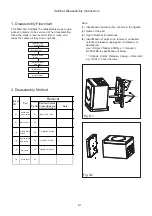
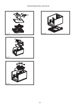
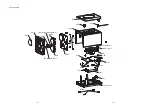
Page 22: ...8 2 Fig D3 Fig D5 Fig D4 Cabinet Disassembly Instructions Fig D6 A02 A03 A04 A02 ...

Page 23: ...ed circuit check and change the related components of radio controlled circuit check if power supply of radio is normal check and change related components of power supply circuit check if radio circuit an components of around it is normal check and change components of around it No No No No No No No sound from whole unit FLOW CHART NO 3 Yes No Yes No Yes no sound from CD check if CD output is nor...

Page 24: ...er head ass y check if laser head ass y can light normally decoding board is broken check if tie wires of laser head ass y is loosen and broken laser head ass y broken Yes check if supply 12V of decoding board is normal no search from CD check steady circuit No ...

Page 25: ...DD LCD DISPLAY 5V 5 6V OPT 4558 BD3490FS FR_OUT AMPLIFIER TDA7491P FL_OUT LCD Driver PT6533 MCU R5F21266 IR IR AD_KEY EEPROM M24C02 M3 3V Apple Ceriticiate CP2 0B STB MUTE STB MUTE TX RX CTL DET KEY 9 4OHM_5W 2 TX RX CTL DET DVD_ON VUSB_ON 9435 CD_5V 8V AMP TDA7491P DC DC AP1534 TRANSFORMER CD DVD_ON GND IGND I5V 3 3V 1117 LDO 7333 MCU3 3V M3 3V ECO IPOD IPHONE 5V 5V PSU BOARD AC220V IPOD IPHONE_5...

Page 26: ...CD Loader driver machanism AC220V Wiring Diagram AMP Board Decoder Board Display Board Power Board PJ3 J6 J3 J4 J2 J1 CON3 J7 PJ2 CON2 CON1 CON4 CON3 J1 JP4 CN1 CON1 CON2 CON1 11 1 11 1 ...

Page 27: ...EG8 SEG7 SEG6 SEG5 SEG4 SEG3 SEG2 SEG1 COM8 COM7 COM6 COM5 COM4 COM3 COM2 COM1 COM01 COM00 SEG00 COM5 COM05 COM04 COM6 COM06 COM7 COM07 COM8 SG29 SG28 SG27 SG26 SG25 SG24 23 SEG22 SEG23 24 25 26 27 28 29 30 31 32 33 SG2 SG3 SG4 SG5 SG6 SG7 SG8 SG9 SG10 SG11 1 2 3 4 5 6 7 8 9 10 11 SEG00 SEG01 SEG02 SEG03 SEG04 SEG05 SEG06 SEG07 SEG08 SEG09 SEG10 DI SG22 SG21 SG20 SG19 SG18 SG17 SG16 SG15 SG14 SG13...

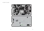
Page 28: ...Display Board Layout Diagram 12 2 12 2 ...

Page 29: ... R19 2 32K 1 0805 R5 2M 1206 D4 1N4007 R7 NC C6 2200uF 10V D11 NC R10 1 2R 1206 R3 2M 1206 D5 NC D6 FR107 R16 3 3K 0805 C2 22uF 50V C1 47uF 400V C3 103P 630V C11 470pF 0805 D7 FR107 R18 12K R13 68R 0805 Q1 4N60 C21 1nF 50V 0805 D9 SB3100 R1 200K 1206 C4 221P 2KV R28 NC R25 330R 0805 C13 NC 1 2 L2 0R 0805 L3 NC IC3 NC SOT23 R23 NC R12 1K 0805 RT 3 CS 4 GND 1 OUT 6 VCC 5 FB 2 IC4 KB8235 SOT23 6 R22 ...

Page 30: ...Power Board Layout Diagram 12 4 12 4 ...

Page 31: ...6 100pF R20 0R C114 2 2uF NC L3 FB 1K C43 100pF C98 2 2UF 1 2 3 4 J7 4P_1 0UP C112 2 2uF CB14 33PF D9 ESD C28 470pF R79 33R R99 100R R1 10R R 0805 R106 3 3R R103 100 R80 2 2k L24 100R 6A 100M R133 10K NC R72 68K C100 0 1uF C87 100pF 1 SUB_GND 22 INPA 23 INNA 27 SGND 26 VDDS 28 DIAG 19 VDDPW 18 PGND 25 SYNCLK 24 ROSC 30 GAIN0 31 GAIN1 35 SVCC 8 OUTNB 4 PGNDB 5 PGNDB 6 PVCCB 7 PVCCB 3 OUTPB 11 OUTNA...

Page 32: ...OP 8 R157 22K Q7 8550 A8V 1 3 2 Q6 BS3904 CE23 220u 25V R136 6 8K L52 100R 5A D15 SK34 D14 SK34 L49 22UH CE20 220u 25V FB1 100R 5A R151 1K R152 10K TP30 C129 0 1uF R156 10K 1 3 2 Q8 BS3904 C127 5V 0 1uF C120 153 L46 100R 5A R140 4 7K R142 47K R147 22K CE21 100u 10V 1 GND 2 IN 3 OUT1 U11 SOT89 NC HT7333 R135 4 7K R150 47K C131 0 1uF R146 10K L51 100R 5A CE19 IPOD_5V 220u 10V CE22 220u 10V C121 0 1u...

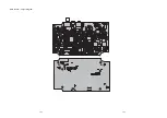
Page 33: ...AMP Board Layout Diagram 12 7 12 7 ...

Page 34: ...F EC17 10uF 16V C33 104 1 2 D4 1N5819 TP4 C47 0 1uF 2 2 3 3 4 4 5 5 9 9 8 8 7 7 6 6 1 1 H2 HOLE GND C21 104 R4 3 9K R25 330R R25 330R L4 DCR33 R38 33R C9 104 C11 104 D5 NC R53 10K R67 10K C42 104 C19 104 C23 30pF TP5 C15 104 EC14 10uF 16V D6 NC RX R45 22K 1 2 D7 IN4001 C35 104 D8 3 3V SMD 2 2 3 3 4 4 5 5 9 9 8 8 7 7 6 6 1 1 H4 HOLE GND R34 15k TP6 CS 1 DO 2 WP 3 GND 4 DI 5 CLK 6 HOLD 7 VCC 8 U3 SF...

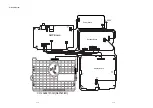
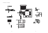
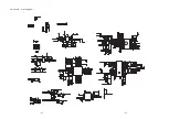
Page 35: ...Decoder Board Layout Diagram 12 9 12 9 ...

Page 36: ...View PCB1 PCB3 S001 Bottom Cover Rubber Foot S008 S005 S011 S009 Light Guide Ringe PMMA SCREW S010 PCB2 PCB4 S007 S003 S012 S006 CD Door Gear Gear Bracket CDM Screw Screw Screw Screw IR Reciver Bracket 13 1 13 1 ...

Page 37: ...Revision List Revision List Version 1 0 Initial Release Version 1 1 Add 12 version ...

Reviews: