background image

LAYOUT DIAGRAM - MCU BOARD

BOTTOM SIDE

9-

3

 9-

3

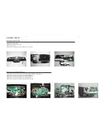
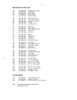
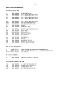
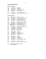
Summary of Contents for MCM330

Page 1: ...rior permission of Philips CONTENTS Technical specification 1 2 Version variation 1 2 Service measurement setup 1 3 Service aids 1 4 Instructions on CD playability 2 1 2 2 Block diagram 3 1 Wiring diagram 4 1 Disassembly diagram 5 1 Power board Circuit diagram 6 1 6 3 Layout diagram 6 4 6 5 CD board Circuit diagram 7 1 Layout diagram 7 2 7 3 Display board Circuit diagram 8 1 Layout diagram 8 2 8 3...

Page 2: ... Standby Power Consumption 2W Eco Power Standby Power Consumption 1W USB Direct Version 2 0 1 1 Dimensions Main Unit W x H x D 571 x143 x 91mm Weight Main Unit 1 91 kg Amplifier Total output power 2X10W RMS with Living Sound off 4 x 6W RMS with Living Sound on Frequency response 125Hz 16kHz 3dB Signal to noise ratio 65dB MP3 link input 0 5 V RMS 20kohm TECHNICAL SPECIFICATION 1 2 Type Versions Fea...

Page 3: ...15kHz e g 7122 707 48001 LF Voltmeter e g PM2534 DUT S N and distortion meter e g Sound Technology ST1700B Frame aerial e g 7122 707 89001 Tuner AM MW LW To avoid atmospheric interference all AM measurements have to be carried out in a Faraday s cage Use a bandpass filter or at least a high pass filter with 250Hz to eliminate hum 50Hz 100Hz RF Generator e g PM5326 Ri 50 Bandpass 250Hz 15kHz e g 71...

Page 4: ...ng make sure that you are connected with the same potential as the mass of the set via a wrist wrap with resistance Keep components and tools also at this potential ESD CLASS 1 LASER PRODUCT GB Safety regulations require that the set be restored to its original condition and that parts which are identical with those specified be used Safety components are marked by the symbol Lead free ...

Page 5: ...T OK check playability N Y playability ok check playability check playability return set Customer complaint CD related problem fast lens cleaning 1 2 3 For flap loaders access to CD drive possible cleaning method 4 is recommended INSTRUCTIONS ON CD PLAYABILITY 2 1 Exchange CDM 1 4 For description see following pages ...

Page 6: ...viously caused by a scratched dirty or copy protected CD In case problems remain the customer is requested to contact the workshop directly The lens cleaning method 3 should be mentioned in the addendum sheet The final wording in national language as well as the printing is under responsibility of the Regional Service Organizations 4 LIQUID LENS CLEANING Because the material of the lens is synthet...

Page 7: ...B SOUND CONTROL SW VOL EQ PT2314 POWER AMP TDA8932 2x10W AUX INTPUT DISPLAY VFD SD USB Device NOR FLASH SST39VF400A SDRAM 16Mbit TUNER FM RDS Si4703 VFD DRIVER PT6324 VFD VOLTAGE Circuit KEY Function LIVING SOUND TL072 LIVING SOUND POWER AMP TDA8932 2X6W AC ADAPTER CD PCB KEY PCB USB PCB MCU PCB POWER PCB DISPLAY VFD PCB USB PCB 3 1 ...

Page 8: ...D VFD BOARD CN4 CN8 CN6 CON3 CON4 CON6 CN1 CN2 J204 J205 CN1 CN01 USB SD CARD BOARD CD BOARD CDM CONNECT BOARD DC JACK BOARD J2 CM3 CN602 CN807 CN804 CM1 CN5 CN401 CON3 CM2 MOTOR SWITCH BOARD IR BOARD CN806 CN402 CN4 CON1 SET WIRING DIAGRAM 4 1 ...

Page 9: ...s B as indicated to loosen the rear cabinet B FRONT CAB REAR CAB CD PART C D E F G 1 Remove 3 screws C as indicated to loosen the Key Board and USB SD jack Board 2 Remove 5 screws D as indicated to loosen the Power Board 3 Remove 2 screws E as indicated to loosen the DC jack Board 4 Remove 4 screws F as indicated to loosen the CD Board 5 Remove 6 screws G as indicated to loosen the CD mechanism ...

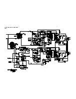
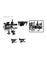
Page 10: ...CIRCUIT DIAGRAM POWER BOARD PART1 6 1 6 1 ...

Page 11: ...CIRCUIT DIAGRAM POWER BOARD PART2 6 2 6 2 ...

Page 12: ...CIRCUIT DIAGRAM POWER BOARD PART3 6 3 6 3 ...

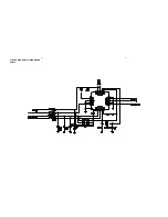
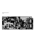
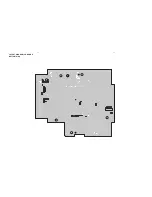
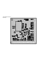
Page 13: ...LAYOUT DIAGRAM POWER BOARD TOP SIDE 6 4 6 4 ...

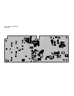
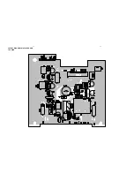
Page 14: ...LAYOUT DIAGRAM POWER BOARD BOTTOM SIDE 6 5 6 5 ...

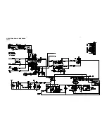
Page 15: ...CIRCUIT DIAGRAM CD BOARD 7 1 7 1 ...

Page 16: ...LAYOUT DIAGRAM CD BOARD TOP SIDE 7 2 7 2 ...

Page 17: ...LAYOUT DIAGRAM CD BOARD BOTTOM SIDE 7 3 7 3 ...

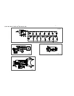
Page 18: ...CIRCUIT DIAGRAM DISPLAY VFD BOARD 8 1 8 1 ...

Page 19: ...LAYOUT DIAGRAM DISPLAY BOARD TOP SIDE 8 2 8 2 ...

Page 20: ...LAYOUT DIAGRAM DISPLAY BOARD BOTTOM SIDE 8 3 8 3 ...

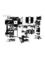
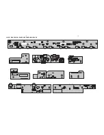
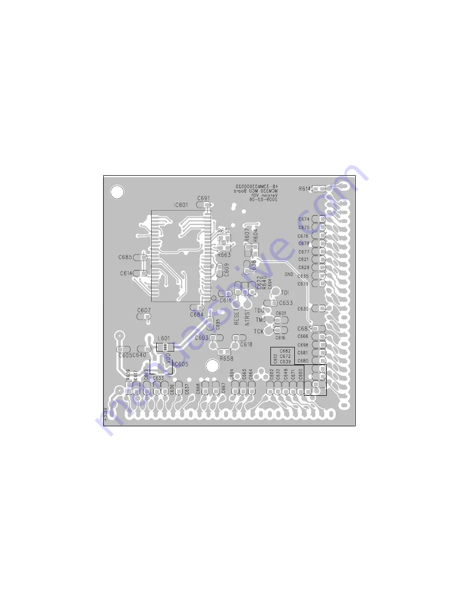
Page 21: ...CIRCUIT DIAGRAM MCU BOARD 9 1 9 1 ...

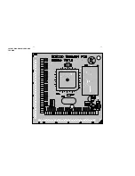
Page 22: ...LAYOUT DIAGRAM MCU BOARD TOP SIDE 9 2 9 2 ...

Page 23: ...LAYOUT DIAGRAM MCU BOARD BOTTOM SIDE 9 3 9 3 ...

Page 24: ...CIRCUIT DIAGRAM KEY BOARD AND SOME SMALL BOARD 10 1 10 1 SD PART USB PART HD OUTPUT PART KEY PART ...

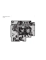
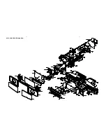
Page 25: ...LAYOUT DIAGRAM KAY BOARD AND SOME SMALL BOARD 10 2 10 2 ...

Page 26: ...SET EXPLODED VIEW DIAGRAM 11 1 11 1 ...

Page 27: ...0023945 USB COVER 220 996510023931 ROLLER BOTTOM GEAR 221 996510023911 ROLLER TOP GEAR 222 996510023901 TOP GEAR 223 996510023939 DRIVER GEAR 1 224 996510023906 TOP BUTTONS 225 996510023913 LED LIGHTGUIDE LENS 226 996510023921 DOOR LENS 228 994000002818 DOOR MOTOR PULLY 229 996510023929 BUTTONS RING 230 996510023951 STAND PC ABS J001 994000001942 16P FFC 1MM L80MM J002 996510023954 8 FFC 1mm L 120...

Page 28: ...01 996510012038 IC TDA8932BT U202 996500039806 IC ET2314 SOP28 U206 994000001201 IC NJM4556AM U59 996510012555 IC 74HC4052D U62 996510019882 IC D4558 U901 996510023943 IC AP1509SL SOP 8 U902 996510023949 IC LM1117S 5V SOT 223 X101 996500042441 X TAL 32 768KHZ 20PPM DISPLAY BOARD ASSEMBLY T1 996510023899 TRANSFORMER only for bare PCB 48 04MM33000320 VFD401 996510023915 VFD DISPLAY KEY BOARD ASSEMBL...

Page 29: ... TRANSISTORS B772Y 160 320 R131 994000004478 FUSE RESISTORS 1R 1W 5 R704 994000004478 FUSE RESISTORS 1R 1W 5 R901 994000004478 FUSE RESISTORS 1R 1W 5 REM1 996510023905 OPTIC SENSER FM 9038TM2 5AN S701 994000004552 DETECT SWITCH S702 994000004552 DETECT SWITCH S703 994000004552 DETECT SWITCH S704 994000004552 DETECT SWITCH U117 996510018962 IC UTC7805 U118 996510018852 IC UTC7808 U501 996510023902 ...

Reviews: