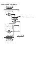
1 - 5
SERVICE AIDS
GB
WARNING
All ICs and many other semi-conductors are
susceptible to electrostatic discharges (ESD).
Careless handling during repair can reduce life
drastically.
When repairing, make sure that you are
connected with the same potential as the mass
of the set via a wrist wrap with resistance.
Keep components and tools also at this
potential.
ESD
CLASS 1
LASER PRODUCT
GB
Safety regulations require that the set be restored to its original
condition and that parts which are identical with those specified,
be used
Safety components are marked by the symbol
!
.
Lead free
Summary of Contents for MCM395/12
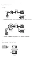
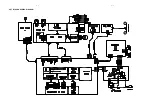
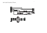
Page 9: ...SET BLOCK WIRING DIAGRAM 3 1 4 1 ...
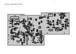
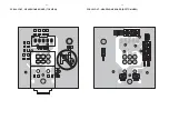
Page 10: ...5 1 5 1 PCB LAYOUT MAIN BOARD TOP VIEW ...
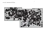
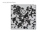
Page 11: ...PCB LAYOUT MAIN BOARD BOTTOM VIEW 5 2 5 2 ...
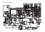
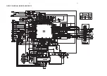
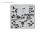
Page 12: ...5 3 5 3 CIRCUIT DIAGRAM MAIN BOARD PART1 ...
Page 13: ...5 4 5 4 CIRCUIT DIAGRAM MAIN BOARD PART2 ...
Page 14: ...5 5 5 5 PCB LAYOUT HEADPHONE BOARD TOP VIEW PCB LAYOUT HEADPHONE BOARD BOTTOM VIEW ...
Page 15: ...5 6 5 6 PCB LAYOUT AUX BOARD TOP VIEW PCB LAYOUT AUX BOARD BOTTOM VIEW ...
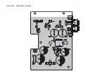
Page 16: ...5 7 5 7 CIRCUIT DIAGRAM HEADPHONE AUX BOARD ...
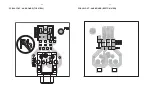
Page 17: ...6 1 6 1 PCB LAYOUT PANEL BOARD TOP VIEW ...
Page 18: ...PCB LAYOUT DISPLAY BOARD BOTTOM VIEW 6 2 6 2 ...
Page 19: ...6 3 6 3 CIRCUIT DIAGRAM PANEL BOARD ...
Page 20: ...7 1 PCB LAYOUT AMP BOARD TOP VIEW 7 1 ...
Page 21: ...7 2 PCB LAYOUT AMP BOARD BOTTOM VIEW 7 2 ...
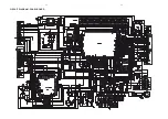
Page 22: ...7 3 CIRCUIT DIAGRAM AMP BOARD 7 3 ...
Page 23: ...8 1 PCB LAYOUT RECTIFIER BOARD TOP VIEW 8 1 ...
Page 24: ...8 2 PCB LAYOUT RECTIFIER BOARD BOTTOM VIEW 8 2 ...
Page 25: ...8 3 CIRCUIT DIAGRAM RECTIFIER BOARD 8 3 ...
Page 26: ...8 4 PCB LAYOUT USB BOARD TOP VIEW 8 4 PCB LAYOUT USB BOARD BOTTOM VIEW ...


