background image

SET BLOCK & WIRING DIAGRAM

3 - 1

4 - 1

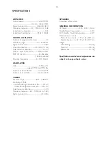
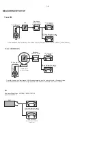
Summary of Contents for MCM395/12

Page 1: ...sion of Philips Published by SL 0822 Service Audio Printed in The Netherlands Subject to modification Micro System Version 1 1 CLASS 1 LASER PRODUCT 3141 785 32501 TABLE OF CONTENTS Page PCBs Location 1 2 Specifications 1 3 Measurement Setup 1 4 Service Aids Safety Instruction etc 1 5 to 1 7 Software Version Checking 2 Set Block Diagram 3 Set Wiring Diagram 4 Main Headphone AUX Board 5 Panel Board...

Page 2: ...tures Voltage Selector ECO Power Standby LCD Display Off USB Direct Type Versions MCM395 Features in used 05 VERSION VARIATIONS Type Versions Board in used MCM395 Service policy MAIN BOARD RECTIFIER BOARD PANEL BOARD ECO POWER BOARD TIPS C Component Lever Repair M Module Lever Repair Used C 12 05 8 5 5 9 1 6 8 5 Feature diffrence AMP BOARD C C C USB BOARD C x x x AUX HP BOARD C C CONNECTION BOARD ...

Page 3: ...MA files Number of albums folders maximum 99 Number of tracks titles maximum 500 TUNER FM wave range 87 5 108 MHz Sensitivity at 75 mono 26 dB signal to noise ratio 2 8 µV stereo 46 dB signal to noise ratio 61 4 µV Total harmonic distortion d 5 Frequency response 63 12500 Hz 3 dB Signal to noise ratio t 50 dBA SPEAKERS 2 way Bass reflex system GENERAL INFORMATION AC Power 220 230V 50 Hz Standby Po...

Page 4: ...7122 707 89001 Tuner AM MW LW To avoid atmospheric interference all AM measurements have to be carried out in a Faraday s cage Use a bandpass filter or at least a high pass filter with 250Hz to eliminate hum 50Hz 100Hz RF Generator e g PM5326 Ri 50 Bandpass 250Hz 15kHz e g 7122 707 48001 LF Voltmeter e g PM2534 DUT RF Generator e g PM5326 S N and distortion meter e g Sound Technology ST1700B Use a...

Page 5: ...ng make sure that you are connected with the same potential as the mass of the set via a wrist wrap with resistance Keep components and tools also at this potential ESD CLASS 1 LASER PRODUCT GB Safety regulations require that the set be restored to its original condition and that parts which are identical with those specified be used Safety components are marked by the symbol Lead free ...

Page 6: ...T OK check playability N Y playability ok check playability check playability return set Customer complaint CD related problem fast lens cleaning 1 2 3 For flap loaders access to CD drive possible cleaning method 4 is recommended INSTRUCTIONS ON CD PLAYABILITY 1 6 Exchange CDM 1 4 For description see following pages ...

Page 7: ...viously caused by a scratched dirty or copy protected CD In case problems remain the customer is requested to contact the workshop directly The lens cleaning method 3 should be mentioned in the addendum sheet The final wording in national language as well as the printing is under responsibility of the Regional Service Organizations 4 LIQUID LENS CLEANING Because the material of the lens is synthet...

Page 8: ...1 MCU version at standby mode press and hold PLAY button at least 5 seconds 2 USB version select source USB press and hold STOP SOURCE buttons at least 5 seconds SOFTWARE VERSION CHECKING 2 1 2 1 ...

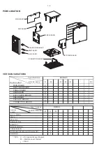
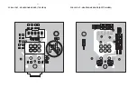
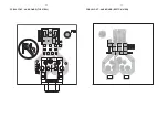
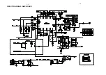
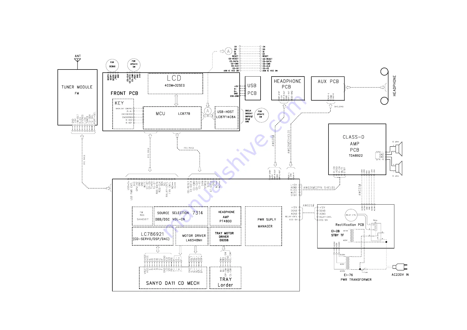
Page 9: ...SET BLOCK WIRING DIAGRAM 3 1 4 1 ...

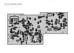
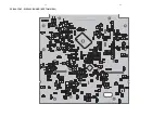
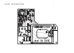
Page 10: ...5 1 5 1 PCB LAYOUT MAIN BOARD TOP VIEW ...

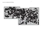
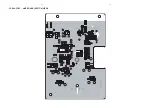
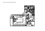
Page 11: ...PCB LAYOUT MAIN BOARD BOTTOM VIEW 5 2 5 2 ...

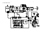
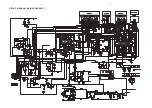
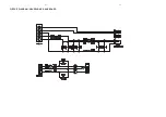
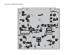
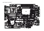
Page 12: ...5 3 5 3 CIRCUIT DIAGRAM MAIN BOARD PART1 ...

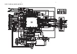
Page 13: ...5 4 5 4 CIRCUIT DIAGRAM MAIN BOARD PART2 ...

Page 14: ...5 5 5 5 PCB LAYOUT HEADPHONE BOARD TOP VIEW PCB LAYOUT HEADPHONE BOARD BOTTOM VIEW ...

Page 15: ...5 6 5 6 PCB LAYOUT AUX BOARD TOP VIEW PCB LAYOUT AUX BOARD BOTTOM VIEW ...

Page 16: ...5 7 5 7 CIRCUIT DIAGRAM HEADPHONE AUX BOARD ...

Page 17: ...6 1 6 1 PCB LAYOUT PANEL BOARD TOP VIEW ...

Page 18: ...PCB LAYOUT DISPLAY BOARD BOTTOM VIEW 6 2 6 2 ...

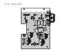
Page 19: ...6 3 6 3 CIRCUIT DIAGRAM PANEL BOARD ...

Page 20: ...7 1 PCB LAYOUT AMP BOARD TOP VIEW 7 1 ...

Page 21: ...7 2 PCB LAYOUT AMP BOARD BOTTOM VIEW 7 2 ...

Page 22: ...7 3 CIRCUIT DIAGRAM AMP BOARD 7 3 ...

Page 23: ...8 1 PCB LAYOUT RECTIFIER BOARD TOP VIEW 8 1 ...

Page 24: ...8 2 PCB LAYOUT RECTIFIER BOARD BOTTOM VIEW 8 2 ...

Page 25: ...8 3 CIRCUIT DIAGRAM RECTIFIER BOARD 8 3 ...

Page 26: ...8 4 PCB LAYOUT USB BOARD TOP VIEW 8 4 PCB LAYOUT USB BOARD BOTTOM VIEW ...

Page 27: ...32 21 27 22 29 7 20 23 31 34 30 4 6 5 1 11 12 3 10 9 2 39 SET MECHANICAL EXPLODED VIEW 9 1 9 1 ...

Page 28: ...30V 50Hz 18 996510011351 REMOTE CONTROL 19 996510005595 PIG TAIL ANTENNA WIRE BLACK 20 996510012801 FRONT CABINET 21 996510012822 CONTROL KNOB PLAY PAUSE 22 996510012802 CONTROL KNOB FB 23 996510012803 CONTROL KNOB PRESETS DOWN 24 996510012823 CONTROL KNOB STOP 25 996510012804 CONTROL KNOB FF 26 996510012805 CONTROL KNOB PRESETS UP 27 996510012806 DISPLAY LENS 28 996510012824 USB DOOR 29 996510012...

Page 29: ...996510012793 TRANSISTOR BC847B F101 996510012796 FUSE 2 5A 250V CSA VDE Q214 994000005755 TRANSISTOR KTA1273 F102 996510012797 FUSE 6 3A 250V 5RT 063H Q215 996510012793 TRANSISTOR BC847B F103 996510012797 FUSE 6 3A 250V 5RT 063H Q3 996510012793 TRANSISTOR BC847B HP902 996510001073 EARPHONE CKX3 5 19S 3PIN Q303 996510012793 TRANSISTOR BC847B IC201 994000005724 IC LD1117AL 3 3V D Q304 996510012793 T...

Page 30: ... ZD1 996510004557 DIODE 5V6 1 2W TCLLZ5V6 LL34 ZD101 996510012789 ZENER DIODE 7V5 ZD101 996510011338 DIODE BZX79 B8V2 SOD27 ZD102 996510004559 DIODE 8V2 1 2W TCLLZ8V2 LL34 ZD102 996510000379 ZENER DIODE 11V 1 2W TC11V ZD2001 996510004556 DIODE 5V1 1 2W TCLLZ5V1 LL34 ZD2002 994000005743 ZENER DIODE 2V7 1 2W ZD201 996510004555 DIODE 10V 1 2W TCLLZ10V LL34 ZD204 996510004556 DIODE 5V1 1 2W TCLLZ5V1 L...

Page 31: ...10 1 REVISION LIST 1 0 Manual 3141 785 32500 Initial Service Manual released 1 1 Manual 3141 785 32501 In this version on Page 1 2 Version Variations added and Page 7 3 AMP Board Circuit Diagram updated ...

Reviews: