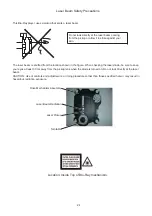
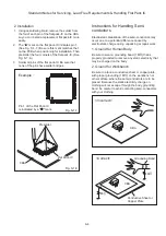

Direction of Use
7-2
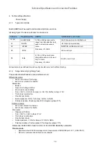
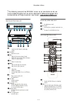
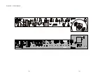
Remote control
3
4
5
6
7
8
9
10
11
12
13
14
15
16
17
18
19
20
21
22
23
SHUFFLE
Play tracks randomly.
SLEEP
Set the sleep timer.
Navigate through menu.
ALBUM/
: Skip to previous/next
album; skip to a preset station.
OK
Con
¿
rmanentryor selection.
Select FM stereo or mono.
RDS/INFO
For selected FM radio stations:
display RDS information.
Display the current status or the disc
information.
Display the ID3 information
(if available) of MP3 tracks.
/
Skip to the previous or next title,
chapter, track, or radio station.
Stop play.
Erase a program.
(In standby mode) Turn on/off Demo
mode.
/
search backwards or forward.
Search to a radio station.
TREBLE / BASS
Activate treble/bass adjustment.
CLOCK
Set the clock.
Display the set clock.
Numeric keypad.
Select a track directly.
SHIFT
Enter a two or three-digit number
(with the numeric keypad).
PROGRAM
Program radio stations.
Program tracks.
VOL +/-
Adjust volume.
Adjust time.
LOUDNESS
Turn on or off automatic loudness
adjustment.
Mute or restore volume.
Start or pause play.
MENU
Access menu.
This button is not workable for this
model.
TIMER
Set alarm timer.
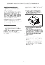
Open or close the disc
compartment.
REPEAT
Select a repeat play mode.
Source buttons
Select a source.
DOCK source is not available for this
unit.
3 Get started
Caution
Use of controls or adjustments or
performance of procedures other than herein
may result in hazardous radiation exposure or
other unsafe operation.
Always follow the instructions in this chapter in
sequence.
If you contact Philips, you will be asked for the
model and serial number of this apparatus.The
model number and serial number are on the
back of the apparatus. Write the numbers here:
Model No. __________________________
Serial No. ___________________________
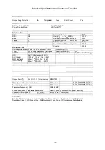
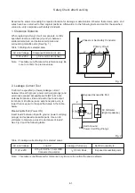
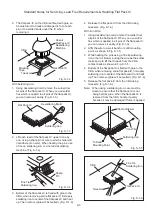
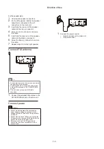
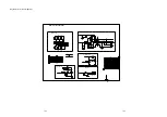
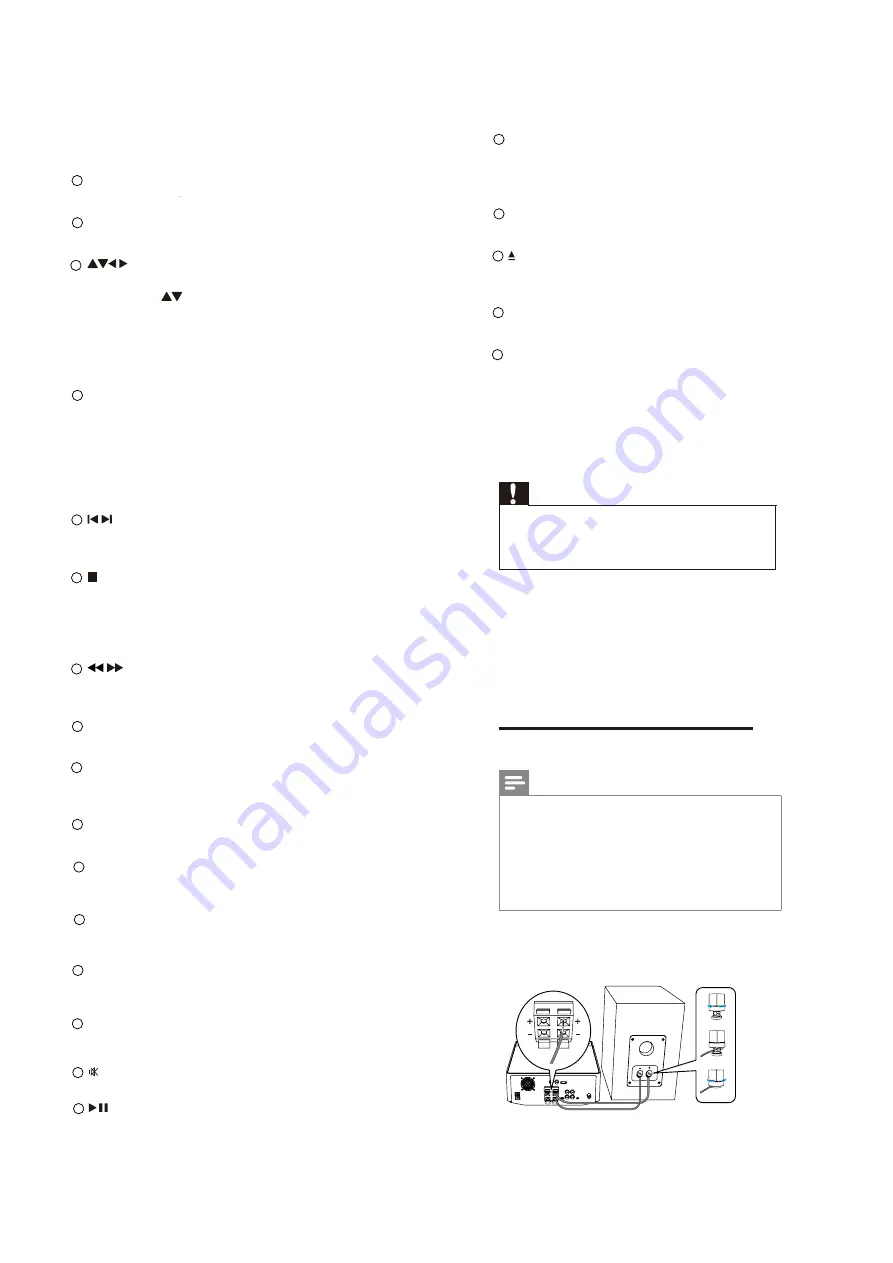
Connect speakers
Note
Ensure that the colors of the speaker wires and
terminals are matched.
For optimal sound, use the supplied speakers
only.
Connect only speakers with impedance that is
the same or higher than the supplied speakers.
Referto the Speci
¿
cations section of this
manual.
For the main unit side:
Connect the speaker wires and the main unit as
the following graphic indicates:
Summary of Contents for MCM7000/12
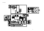
Page 30: ...AMP BOARD Layout Diagram 12 2 12 2 ...
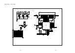
Page 32: ...Display Board Layout Diagram 12 4 12 4 ...
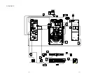
Page 35: ...Key Board Layout Diagram 12 7 12 7 ...
Page 38: ...T5AH 250V Power Board Layout Diagram 12 10 12 10 ...
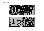
Page 42: ...Decoder Board Layout Diagram 12 14 12 14 ...
Page 44: ...Revision List Revision List Version 1 0 Initial Release 14 1 ...


