background image

‡ ‡ ‡ ‡

TO MCU

TO MCU

AUX IN/LINE OUT

TO MPEG PCB

TO DISPLAY PC

B

TO POWER PC

B

MCU

AGND

AGND

OPEN/CLOSE_SW

CEC_OUTPUT

GND

T

E

S

E

R

T

E

S

E

R

SDA

M_CLOSE

M_CLOSE

CEC_INPUT

M_OPEN

3.3V/GND/I_VIDEO_SW

GND

CEC_OUTPUT

3.3V/I2C_INT

SDA

CD_MUTE

GND

DVD_ON

MBD7020

SDA

N

O

_

D

V

D

N

O

_

D

V

D

3.3V/GND/I_VIDEO_SW

M_OPEN

SCL

3.3V/GND/I_VIDEO_SW

CD_MUTE

HPD

1.0/12P

CD_MUTE

CEC_INPUT

I2C_INT/3.3V

1.0/16P

GND

RESET

MCU <=> MPEG

GND

CD_TRIN

HPD

DCD7010

CD_TRIN

SCL

1.0/12P

MCM7000

SCL

OPEN/CLOSE_SW

GND

1
2
3
4

16

Pins

5
6
7
8
9
10
11
12
13
14
15

FL O+

MSD A

MSC L

FR O-

FR -

PW M_ R ST

FL O-

OT W

LR C K_AD

FR +

OT W

IO_ VD D _C

1.8 V_C

1.8 V_C

MU TE_ 98 31

BC K_AD

A_M U TE

MC U _M U TE

FAN _C TR L

D VD _O N

MO D E

H

D

MI

_HP

D

_

MC

U

MSC L

MSD A

EC O_ POW ER

MSD A

PW

M_R

ST

MC U _M U TE

XC OU T

R

EMOTE

BC K_D VD
LR C K_D VD
D ATA_ D VD

/SD

MC LK_ AD

AU X_IN R

AU X_IN L

AGN D

BC K_D VD
LR C K_D VD
D ATA_ D VD

R

_

P

H

L

_

P

H

DA

T

A

_

D

V

D

BC

K_D

VD

LRC

K_D

V

D

DC5

V

+12

V

P25V

EC

O_POW

ER

FR O+

ZER 0_ LIN E_O U T

R EC OU T_ M_ R

R EC OU T_ P_R

R EC OU T_ M1 _L

R EC OU T_ P1_ L

LIN E_O _L

R

E

C

O

U

T_M

R EC OU T_ M1 _L

R EC OU T_ P1_ L

R

E

C

O

U

T_P

R EC OU T_ M_ R

ZER 0_ LIN E_O U T

SC L1

SD A1

MSC L

MSD A

CS

5

3

4

6

_

R

S

T

M_C

LOSE

H

P

/LIN

E_MU

TE

OTW

CP

_

S

D

A

FAN _C TR L

FL O+

FR O-

FL O-

FL -

AMP_ R ST

AMP_ PD N

FR O+

PW M_ H P_L _P

PW M_ H P_L _M

H P_L AA

PW M_ H P_R _M

PW M_ H P_R _P

MSC L

IPod _R _C H

IPod _L _C H

IPOD _AU D IO_ D ET

S

N

E

S

-

P

H

S

N

E

S

-

P

H

IPOD _D ET

GN D

SGN D

+1 2V

E

T

U

M

1

3

8

9

_

E

T

U

M

FM_ INL

R

N

I

_

M

F

H

C

_

R

_

M

F

FM_ L_ C H

IPod _R _C H

H

C

_

L

_

d

o

P

I

D

O

P

I

_

H

C

L

R C H _IPO D

AU X_IN L

R

N

I

_

X

U

A

H

C

_

R

_

X

U

A

AU X_L _C H

LED _PW M_ VOL

MU TE_ H P/LIN E

VI

D

EO_SW

M_ OPEN

HP

-S

E

N

S

ipod

/D

AB

_TX

ipod

/D

AB

_RX

VFD

-CLK

VFD

-DA

T

A

VFD

-STB

BC K_AD

MP3 _L _C H

MSD A

C S53 46 _R ST

AU X_R _C H

LR C K_AD

MSC L

AU X_L _C H

LC H _IPO D

FM_ R _C H

MC LK_ AD

R C H _IPO D

D ATA_ AD

MP3 _R _C H

FM_ L_ C H

GN D

EC O_ POW ER

VFD -ST B

VFD -C LK

VFD -D ATA

R OT -A/B

H P_R

MP3 _IN R

H P_L

MP3 _IN L

LIN E_O U T_ R

LIN E_O U T_ L

R EMO TE

R

EMOTE

US

B

_

E

N

1

#

U

S

B

_OC1#

IIC

_IN

T

TR

IN

IPOD _AU D IO_ D ET

XOU T

IP

OD_A

C

C

_PW

R

_DE

T

XC OU T

XC IAN

C EC _O U T

XC IAN

C EC _IN PU T

R EST_ MC U

XIN

C P_SC L

H P/LIN E_M U TE

E

T

U

M

_

A

E

N

I

L

/

P

H

_

E

T

U

M

IPod _L _C H

IGN D
ipo d/D AB_T X
GN D
IPod _R _C H

+IP5 V
ipo d/D AB_R X

D AB_M U TE

D AB_M U TE

EC O_ POW ER

MSC L
MSD A

MP3 _L _C H

MP3 _IN L

MP3 _R _C H

MP3 _IN R

LIN E_O _R

IPOD _AU D IO_ D ET

FL +

R

E

C

O

U

T_P1

R

E

C

O

U

T_M1

LIN E_O U T_ R

LIN E_O U T_ L

IR

IR

M_BOY

AMP

_RS

T

AM

P_R

ST

DV

D

_

R

S

T

FM_C

P_R

ST

R

OT-A/B

SS

D

A

SS

C

L

SSC L

SSD A

LED _PW M_ VOL

C P_SC L

C P_SD A

LED _PW M_ VOL

FM_C

P_R

ST

FM_ C P_R ST

SC L3

ipo d/D AB_T X

FM_ INR
FM_ INL

ipo d/D AB_R X

FM5 V

SD A3

D AB_M U TE

SGN D

R

OT-A/B

OPE

N

/C

L_SW

OPE

N

/C

L_SW

M_ BOY

GN D

MC U _5 V

GN D

GN D

GN D

P25 V
P25 V

+1 2V
D C 5V
MC U _5 V

AGN D

GN D

GN D

I2C _IN T/3.3 V

3.3 V/GN D /VID EO_ SW

3.3 V_M C U

3.3 V_M C U

VIDEO _SW

IIC _IN T

D VD _R ST

SSD A

3.3 V/GN D /VID EO_ SW

SSC L

C EC _IN PU T

GN D

A_M U TE

I2C _IN T/3.3 V

GN D

M_ OPEN

TR IN

M_ C LO SE

C EC _O U T

D VD _O N

OPEN /CL _SW

H D MI_H PD _M C U

D ATA_ AD

PW M_ H P_L _P

PW M_ H P_L _M

PW M_ H P_R _P

PW M_ H P_R _M

R EC OU T_ P_R

H P_R AA

MC

U

_5V

P25V

C S53 46 _R ST

MSC L
MSD A

HP

-S

E

N

S

+3 V3

P28 V

+3 V3

+1 2V

P25 V

3.3 V_M C U

3.3 V_M C U

+3 V3

+3 V3

3.3 V_M C U

+3 V3

D C 5V

3.3 V_M C U

MC U _5 V

3.3 V_M C U

+3 V3

3.3 V_M C U

+1 2V

VC C _AM P

VC C _AM P

A5V

A5V

A5V

A5V

+5 V_VA

3.3 V_VD

+5 V_VA

3.3 V_VD

+3 V3

A5V

VLS

3.3 V_VD

3.3 V_M C U

A5V

A5V MC U _5 V

+5 V_VA

3.3 V_M C U

R 20
22 K

R 11 0

15 K

C 62

10 4

R

187

10K/10K/

N

C

C 50

10 4

C 15 7

4.7 U F/16 V

R 94

33 K

R 13 5

47 K

R2

2

6

4

7

0

R 35
6.2 R

C1

3

9

1

0

0

P

R 32 22 K

C B2

10 3

C 12 8

10 3

L6

FB/1K

C 18 2
0.1 uF

D 23
2V

1

2

FB8 FB/08 05 /1K

J 5

C ON 1.0 -4

1

2

3

4

C

2

05

102

R 17 5

33 0/N C

C 52

10 4

C 18 9

0.1 uF

+

C E5
10 0u F/10 V

C B1

10 4

R 56
10 K

P1

PR C -2 01 A
C ON 2.5 4- 4

2

3

1

4

D 15

1N 41 48

1

2

C

2

03

104

C 53

10 2

R

1

48

10K

TP36

FB6

FB/06 03 /12 0R

C 14 6

1u F

R 27

10 K

R 21 1

10 K

C2

1

7

1

0

0

P

C 11 0

10 3

C 19 4

33 2

C 57

10 4

C 11 7

10 3

R 21 2

2.2 K

C 22

10 4

J 1

C ON 2.5 4- 2

1
2

C 15 0

20 pF

C 17 8

0.0 1u F

R 10 22 K

R 15 4
10 K

FB9

FB/08 05 /1K

R 79
6.8 K

C 18 1
0.1 uF

R1

6

2

3

3

C

1

99

332

R 13 7

6.8 K

TP42

J 3
C ON 2.0 -4

1
2
3
4

J 4
C ON 2.0 -4

1
2
3
4

R 43

10 0

U2

PS9831

1

3

5

4

6
7
8
9

10
11
12
13
14
15
16
17
18
19
20
21
22
23
24
25

26

27

28

29

30

31

32

33

34

35

36

37

38

39

40

41

42

43

44

45

46

47

48

49

50

51

52

53

54

55

56

57

58

59

60

61

62

63

64

65

66

67

68

69

70

71

72

73

74

75

76

77

78

79

80

81

82

83

84

85

86

87

88

89

90

91

92

93

94

95

96

97

98

99

100

2

IO_ VSS

PLL _D VD D

IO_ VSS

IO_ VD D

PLL _AVD D
IO_ VSS
PLL _AVSS
IO_ VSS
IO_ VD D
MBC K
ML R C K
D VD D
D VSS
MSD IN0
MSD IN1
MSD IN2
MSD IN3
SBC K
SLR C K
IO_ VSS
IO_ VD D
SSD IN0
SSD IN1
SSD IN2

SS

D

IN

3

EX

T_MU

TE

IO_VS

S

IO_VD

D

MI

C

_

MC

LK

MI

C

_

BC

K

MI

C

_LRC

K

MI

C

_

SD

IN

DV

D

D

DV

S

S

PW

M_SW

_LIN

E_M

PW

M_SW

_LIN

E_P

IO_VS

S

IO_VD

D

PW

M_H

P_R

IGH

T_M

PW

M_H

P_R

IGH

T_P

DV

D

D

DV

S

S

IO_VS

S

PW

M_H

P_LEFT_M

P

_

T

F

E

L

_

P

H

_

M

W

P

IO_VD

D

R

E

C

OUT

_M

R

E

C

OUT

_P

IO_VS

S

R EC OU T_ M

R EC OU T_ P

IO_ VSS

N C

N C

IO_ VD D

IO_ VSS

N C

N C

IO_ VSS

PW M1 _M

PW M1 _P

D VSS

IO_ VSS

IO_ VD D

D VD D

PW M2 _M

PW M2 _P

IO_ VSS

PW M3 _M

PW M3 _P

IO_ VD D

IO_ VSS

PW M4 _M

PW M4 _P

Overload

EP

D

_

EN

A

IO_SO_SD

A

SC

K_SC

L

DV

D

D

DV

S

S

SI

_I2C

_AD

0

N

_

CS

_I2C

_AD

2

SP

_I2C

IO_VS

S

X_I

N

X_OU

T

D

M

IX_LR

C

K

D

M

IX_BC

K

D

M

IX_SD

OUT

DV

D

D

DV

SS

D

M

IX_MC

LK

IO_VD

D

IO_VS

S

NRE

S

E

T

TES

T_MODE

1

TES

T_MODE

2

SC

AN

_EN

A

TES

T_MODE

3

PLL _D VSS

C 93

10 0p F/J

R 10 8
10 K

L4

FB/1K

D 1

1N 41 48

1

2

R

163

100

/100/N

C

R 12 4

18 K

R 63

15 K

C

2

15

100

0P

C 24

47 4

C

2

28

N

C

/100P

L3 3

FB/1K

TP30

L4 1

FB/1K

MAR

K1

R 37

10 0

C2

2

4

1

0

0

P

TP28

Q5
80 50 ,DIP

2

1

3

L26

FB/

1

K

TP29

C 19
XXX-> 47 0P

TP2

R 13 8
18 K

+

C E11

C D 11 X/10 U F1 6V/D 5H 11

R 11
10 0

TP5 7

R 24 0

33 0

+

C 63

47 0u F/16 V

C 11 2
10 3

C 21

10 4

C 42

10 4

R 34
10 R

C ON 3

C ON 2.5 4- 9

1
2
3
4
5
6
7
8
9

R 16 7 2K2

C 17 6

2.2 U F

R 21 6

10 K

L4 8 FB1 00 /5A

+

C 61

22 0u F/16 V

R 20 4

10 K

R 76
10 K

C 28

10 2

Q3
39 04

1

3

2

C 30

10 4

L5 3

FB/1K

R 7
4K7

TP6 5

R 52

1R /08 05

R 16

12 K

TP6 0

R

203

10K

TP5 5

TP5 0

R 17 6

33 0

+

C E19

C D 11 X/22 0U F1 6V/D 5H 11

C 16

10 4

C 20 0

33 2

R2

3

3

NC/

4

7

0

/N

C

C 48

47 4

U 1

TAS5 34 2L

1

3

4

2

5

6

8

17

9

11

10

13

14

15

12

19

18

7

16

20

22

21

24

25

26

28

29

30

31

36

32

35

34

33

41

40

39

42

43

23

27

37

38

44

GVD D _B

N C

N C

/OTW

/SD

PW M_ A

PW M_ B

/RESET _C D

OC _AD J

AGN D

GN D

M3

M2

M1

VR EG

N C

PW M_ D

/RESET _AB

PW M_ C

N C

GVD D _C

VD D

BST_ D

N C

PVD D _D

OU T_ D

GN D _D

GN D _C

OU T_ C

OU T_ B

PVD D _C

PVD D _B

BST_ B

BST_ C

PVD D _A

PVD D _A

OU T_ A

N C

BST_ A

GVD D _D

PVD D _D

GN D _B

GN D _A

GVD D _A

C 16 3

22 2

R 13 9

0

C 18

10 2

R 25 1

47 K

R 90

6.8 K

C ON 7

C ON 2.0 -7

1
2
3
4
5
6
7

C 84

15 0P

R 17 2

10 K

L5

TC 09 03 -1 00 U H  3A

2
4

1
3

TP47

C2

1

6

1

0

0

P

C

2

06

102

R 19 7

47 0

TP40

+

C E14

C D 11 X/10 U F1 6V/D 5H 11

C 35

10 0P

C2

2

3

1

0

0

P

R 57
33 k

C 56

10 4

R 80

15 K

L1 3 1

C 2

10 4

C 15

68 0PF

L5 9

FB/60 0

C 16 1

2.2 U F

C 1

C D 26 3/1 00 0u F/35 V

R2

2

7

3

3

0

C 11

10 4

R 36

10 0

R

1

58

100

+

C E3
10 0u F/16 V

R 21 0

0

C 13 6

33 0p F/J

C 96

1u F

TP20

R 13 6

47 K

C 15 1

20 pF

U 10 C X11 17 -3 .3

SOT 22 3

1

3

4

2

AD

J

IN

OU T2

OU T1

C 12 3

10 3

D 12
ESD /NC

1

2

FB3 FB/08 05 /33 R

R 15 6

47 K

L7

FB/1K

Q6

85 50 ,DIP

2

1

3

C 11 3

10 3

/RST
SEN
SCL
SDA

FM5V

GND

ROUT
LOUT

GPIO2

J 2

TU N ER

FMZ Z- 9P

1
2
3
4
5
6
7
8
9

10
11
12
13

D 10

IN6 0

1

2

R 85
33 K

+

C E24
10 uF /16 v

C 10

47 uF /25 V

R 17 1

10 K

TP31

R 25 5

10 K

MAR

K2

C 11 4

10 3

L5 1

FB/1K

C 10 2

1u F

R 26 6

33 0

C2

0

9

1

0

0

P

TP35

C 19 7

33 2

C 66

10 5

Q4

85 50 ,DIP

2

1

3

R 19 6

33 0

R 26 8

33 0

R 44

27 k

C2

2

2

1

0

0

P

R 82

N C /NC /0

R 12 9

47 K

C 11 5 10 00 pF

R 25

10 0

FB2 FB/08 05 /33 R

R 24 1 10 K

C 83

15 0P

C 11 9

10 3

R 10 3

47 R

C 31

68 0PF

R 12 3

18 K

U 8

R 5F 21 25 8
R 8C 24 25 -L QF P52

1

2

3

4

5

6

7

8

9

10

15

13

16

17

18

19

20

21

22

23

30

31

32

33

34

35

36

37

38

39

43

44

45

46

47

48

49

50

51

52

11

24

29

42

12

14

25

26

28

27

41

40

N C

SC LK

D VD _O N

SSD A

MO D E

XC IAN

XC OU T

R ST

XOU T

VSS

OPE

N

_SW

M_ OPEN

C

LOSE_SW

VFD

_CLK

VFD

_DA

T

A

VFD

_STB

R

E

M

OTE

R

O

TB2

R

O

TA2

TX1

D AB_SW

STAN D BY

MU TE_ MC U

MU TE_ LIN E

LED _C TR L

EC O_ POW ER

MSD A

MSC L

AD 0

N C

AD

3

AD

_VR

EF

TR

EO

IP

OD_S

W

SD

_DE

T

AD

4

AD

5

AD

6

US

B

_

D

E

T

D

V

D

_SW

XIN

RX

1

TX2 (R OT A3)

AD

2

VC C

M_C

LOSE

R

OTA1

NC

R X2( R OT B3)

R OT B1

AD

1

NC

R 65 10 0k

C 36

10 0P

C 16 6

10 4

R 25 2

47 K

C 12 6

22 0u F/16 V

R 16 4

10 0R

C 38

33 3

R 21
10 K

L1 0 10 uH 5A

R 14 6

10 K

R 19 1

33 0

C 20

47 uF /16 V

L2 2

N C /FB-1 K/NC

R 99
10 K

C 7

10 4

C2

2

5

1

0

0

P

C

1

32

104

TP25

C B9
0.1 uF

R 3 1K

R 10 5

10 K

L25

FB/

1

K

Q1 2
80 50

2

1

3

R 22 2

N C /10 K/NC

R 49
6.2 R

R 10 4

10 K

C2

1

1

1

0

0

P

C 14 5

0.1 uF

L4 9

FB1 00 /5A

TP5

U 11
24 C 02

1

2

3

4

5
6
7
8

A0

A1

A2

A

D

S

S

S

V

SC L
TEST
VD D

+

C E18

C D 11 X/22 0U F1 6V/D 5H 11

C

2

29

N

C

/100P

+

C E9
C D 11 X/10 U F1 6V/D 5H 11

C2

2

1

1

0

0

P

R 23 6

10 K

C 29

47 uF /16 V

TP6 7

C 91

10 0p F/J

R 17 7

1k

C 16 5

10 4

R 10 2

33 K

R 89

33 K

C

2

08

102

MAR

K3

Q1 3
80 50

2

1

3

R 14 2K7

R 24 4

1K

C 15 9

2.2 uF

C 19 2
10 1

C 13 7

82 P

+C E1

C D 11 X/10 0U F1 6V/D 6.3 H 7

L6 0

FB/60 0

R

1

61

100

L2 1

N C /FB-1 K/NC

+ C E13

C D 11 X/47 0U F1 6V/D 5H 11

TP6 3

R2

1

4

NC/

N

C

/3

3

R 10 7

47 R

R 87

6.8 K

+

C E26

10 0u F/10 V

R 71

15 K

R 12 6

0R

R 83

0/0 /NC

C B8

0.1 uF

C2

2

0

1

0

0

P

R 93

6.8 K

R 46
6.2 R

D 2
BAS31 6

1

2

R 24 5 10 K

R2

2

8

3

3

R 26 9
3.3 K

C 9

10 4

TP32

L1

10 uH 5A

R2

3

2

3

3

0

R 26 7

33 0

TP46

C 15 8
0.1 uF

R 17 9

0R /NC /NC

C 39

10 4

R 16 9

FB6 00

TP7 0

+

C E10

C D 11 X/10 U F1 6V/D 5H 11

C 54

68 0PF

R 14 3

10 K

C

1

90

332

C

B

7

0.1uF

+ C E21

N C /2.2u F/50 v

R 26
10 K

C 13

10 4/2 01 2

+

C E25
47 uF /16 v

C 55

33 3

TP6 6

L1 8

FB/1K

C 19 3

10 1

P2

1

2

3

4

5

6

R 21 7

10 K

R 1

47 K

R 16 5

3.9 K

L1 5 FB

C2

1

9

1

0

0

P

C 17

33 3

R 9 10 0

TP5 3

MAR

K4

C2

0

4

1

0

0

P

-

+

U 3B
45 58 /SO

5

6

7

8

4

R

2

65

100

C 16 8

10 4

C 3

0.1 uF

C 86 56 P

C 16 0

2.2 uF

R 4 1K

R 24 8

1K

FB5 FB/06 03 /12 0R

L3 1

N C

R 53

10 R

+

C E23

1U F

L3 4

FB/1K

C

2

31

104

R 13 4

6.8 K

U 7

C S53 46
LQ FP- 48 L

1
2
3
4
5
6
7
8
9

10
11
12

13

14

15

16

18

19

20

17

21

22

23

24

25

26

27

28

29

30

31

32

33

34

35

36

37

38

39

40

41

42

43

44

45

46

47

48

SD A/CD OU T
SC L/C C LK
AD 0/C S
AD 1/C D IN
VLC
R ST
AIN3 A
AIN3 B
AIN2 A
AIN2 B
AIN1 A
AIN1 B

AGN

D

VA

AFI

LTA

AFI

LTB

VQ

FILT+

NC

VQ

A

IN4

A

/M

ICI

N

1

A

IN4

B

/M

ICI

N

2

AI

N

5

A

AI

N

5

B

MIC BIAS

AIN6 A

AIN6 B

PGAO U TA

PGAO U TB

N C

N C

AGN D

N C

N C

N C

VLS

NC

NC

NC

NC

SD

OUT

SC

LK

LRC

K

MC

LK

D

GND

VD

IN

T

OVFL

L3 6

FB/1K

C 23

10 2

R 68

22 0k

C B6

0.1 uF

TP26

R 10 1

33 K

R 88

33 K

C1

4

0

1

0

0

P

R 95

33 K

C 17 1

4.7 U F/16 V

R 15

10 K

C2

1

8

1

0

0

P

R 20 9 0/0 80 5

L3 8

FB/1K

C 69

33 0P

R 12 7

10 0R

C 64

1u

C 19 6

33 2

R 29

10

C 18 0

N C /10 0P/N C

+

C E16

C D 11 X/10 U F1 6V/D 5H 11

R 19 3 N C /33 0

C 65
10 4

TP5 9

C ON 6

C ON 2.0 -4

1

2

3

4

L2

10 uH 5A

R 81

15 K

Q2
80 50

2

1

3

R 27 3
1K

R 23 9

33 0

R

1

22

10K

C 10 0

1u F

TP51

R 41

10 0

C 17 4

2.2 uF

C 14 1

4.7 uF

D 13

1N 41 48

1

2

C 4

22 P

R 18

10 0

R 55 33 k

C 14 7

10 4

4

0

1

4

1

C

L24

FB/

1

K

R 21 3

0

R 64

0

R 18 2

10 0

R

1

83

10K

C 43

C 49

22 4( 2)

22 4( 2)

R2

3

0

3

3

0

R 19 5

N C /NC /NC /10 0R

R 14 0
18 K

L4 0

FB/1K

D 20

1N 41 48

1

2

C 15 3

10 0p F

FB1 0

FB/06 03 /1K

C 14 2
0.1 uF

+

C E22

C187

332

C186

332

C184

100P

C183

100P

10 0u F/1O V

L27

FB/

1

K

R 12 1

1R

R 20 2

68 K

L1 4

FB

TP4

C 17 0

4.7 U F/16 V

U 9

C X11 17 -3 .3

SOT 22 3

1

3

4

2

AD

J

IN

OU T2

OU T1

C 41

68 0PF

R 20 0
4.7 K

TP27

R 40
6.2 R

C 16 4

22 2

C 44

10 2

L2 0

FB/1K

FB7 FB/08 05 /12 0R

R 17

82 /1W

C 13 3

82 P

+

C E29

10 0u F/10 v

L2 9

FB/1K

TP6 9

R 23 5
N C /10 K/NC

C 6

10 3

C 25

22 4( 2)

C 70

33 0P

L4 5

FB/1K

R 12 0

1R

C 15 5

4.7 U F/16 V

C 12 4

10 4

C 71

10 4

C 15 4

4.7 U F/16 V

+

C E6

C D 11 X/10 U F1 6V/D 5H 11

U 6

D R V60 4

C S84 15 -T SSOP2 8

1

2

3

4

5

6

7

8

9

10

11

12

13

14

15

16

17

18

19

20

21

22

23

24

25

26

27

28

+L D _L

-L D _L

OU T_ LD L

AGN D

EN _L D

PVSS_L D

C N _L D

C N _H P

PVSS_H P

EN _H P

AGN D

OU T_ H PL

-H P_L

R

_

P

H

+

L

_

P

H

+

-H P_R

OU T_ H PR

N C

PGN D

PVD D _H P

C P_H P

C P_L D

PVD D _L D

PGN D

EX_U VP

OU T_ LD R

-L D _R

+L D _R

R 25 4
10 K

R 13 2

10 0R

TP21

C 17 5

2.2 uF

Y1

*1 2.2 88 MH z

TP45

R 21 5

2.2 K

TP22

C 11 6

10 00 P

L28

FB/

1

K

R

2

21

470

C 27

10 4

U 12

D 27 61

1

2

3

4

5

6

7

8

9

10

V+

OU TA

INA

INT

VR EF

SEN C E

SW

INB

OU TB

GN D

C 51
XXX-> 47 0P

R 11 8

15 K

R 15 2

10 K

TP5 6

TP52

R 48
10 R

R 27 1
N C /4.7K

R 66

0

R 38
10 R

R 24 2 10 K

R 19 4

N C /33 0

C 5

22 P

FB1

FB/08 05 /12 0R

R 13 1

6.8 K

D 8

1N 41 48

1

2

TP44

R 62
10 0k

R 13 3

10 0R

R 14 7

10 K

C 32

22 4( 2)

C 75

33 0P

TP5 4

R 6
4K7

C 13 4

82 P

D 3
BAS31 6

1

2

C

1

91

332

R 19 9

33 0

C 21 4 0.1 uF

R 10 6

10 K

C

1

27

104

R 61

10 0k

R 26 3

N C /47 0/N C

L1 1 FB

TP6 2

R

2

08

10K

R 24
10 K

R 54

10 (3 )

R 26 0

10 K

C 34

10 0P

R 31

10

R2

2

9

3

3

0

/N

C

C 46

10 4

Y2
32 .76 8KH z

L4 2

FB/1K

R 19 8

1K

R

155

TP1

C 14 8

C 73

33 0P

C 33

10 4

L3 2

FB/1K

C 18 5
10 1

R 14 2
10 K

R 96

6.8 K

L1 7

FB/60 0

C 14 3
1u F

R2

2

5

4

7

0

C N 6

6x 2.0  W/H OU SING

FPC 16 P

6

5

4

3

2

1

7
8
9
10
11
12
13
14
15
16

FB1 1

FB/08 05 /12 0R

C 15 2

10 0p F

+ C E2

10 0U F1 6V/D 6.3 H 7

R 23

12 K

D 16
ESD /NC

1

2

R 11 9
3.9 K

R 18 5

33

Q1 1
2N 39 04

2

1

3

R 10 0

N C /NC /NC

R 51

47 0

L5 4

FB/1K

TP41

C

2

12

104

/104/N

C

C 17 7

0.0 1u F

+

C E27
47 uF /16 V

C 16 7

08 05 /4.7u F/10 V

TP24

C 45
XXX-> 47 0P

R 15 0

10 0R

D 18

ESD /NC

1

2

R 70

0

R

1

74

330

/330/N

C

R 39

10 0

TP39

R 17 8

10 0

R 24 6 10 K

D 19

1N 41 48

1

2

R 47

10 K

L4 6

FB/1K

R

2

74

10K

C

2

26

N

C

/100P

L5 6

FB/1K

C 76

33 0P

C 79

2.2 uF

+

C E7

C D 11 X/10 U F1 6V/D 5H 11

+

C E17

C D 11 X/10 U F1 6V/D 5H 11

R 45
10 R

TP33

H 1

SYP58 0

R

1

60

330

R

1

49

10K

TP6 8

C 16 9

4.7 U F/16 V

TP3

R 15 1

10 0R

C 67

10 3

R 27 0
4.7 K

C

2

07

102

C 17 2

4.7 U F/16 V

R 8 4.7  1W

+

C E20

10 0u F/10 v

R 69
3.3

C 15 6

4.7 U F/16 V

C 12 2

10 3

C

2

30

104

R 18 4

N C /NC /0R

C N 1

C ON 1.0 -1 2

1
2
3
4
5
6
7
8
9
10
11
12

1
2
3
4
5
6
7
8
9

10
11
12

C N 2

D IN9 /NC /DIN 9

1
2
3
4
5
6
7
8
9

1
2
3
4
5
6
7
8
9

FB4

FB/08 05 /12 0R

R

1

57

100

C

2

13

332

R2

2

3

1

K

/1

K

/NC

R 25 3

10 K

C 74

33 0P

+

C 8
10 0U F1 6V/D 6.3 H 7

C 81

56 P

R 78

22 K

C 19 5

33 2

C 11 8

10 3

C 26

XXX-> 47 0P

C 11 1

10 3

L5 5

FB/1K

C2

0

2

1

0

0

p

R 12
10 K

C2

1

0

1

0

0

P

C 12 1

10 4

L4 3
FB1 00 /5A

L9

FB

TP37

C 10 1

10 uF /10 V/08 05

R 22

1K

L1 6

FB/1K

R 42

10 0

C 13 5

33 0p F/J

R 72

0

C 72
10 5

R 18 6

33 0

R 33

1K

R 20 7

N C /NC /NC /10 0R

R 92

15 K

TP6

C 68

10 5

C 37

10 0P

R 23 7

10 K

+

C E8

C D 11 X/10 U F1 6V/D 5H 11

C 78

33 0P

R 2

3.3

D 9

1N 41 48

1

2

R 25 9

10 K

TP5 8

C ON 1

ST- 01 3

1

2

R

2

31

330

R 13
10 K

R2

3

4

NC/

N

C

/3

3

-

+

U 3A
45 58 /SO

3

2

1

8

4

TP4 9

C 20 1

33 2

TP48

C 14 9

08 05 /4.7u F/10 V

R 73

N C /NC /0

C 12

22 0u F/16 V

TP23

L3 0

FB/1K

R 12 8

6.8 K

C 17 9

N C /10 0P/N C

R 27 2 1K

TP43

R 30

N C

R 19

10 0

TP6 4

C 77

47 1p

L8

10 uH 5A

R

1

59

100

D 22

ESD /NC

1

2

L2 3

FB/1K

R 84

33 K

C 95

1u F

C 16 2

10 4

C

2

27

N

C

/100P

C 85

56 P

+

C E30

22 0u F/10 V

L4 4

FB/1K

C 82 56 P

R 28
10 K

L3 7

FB/1K

D 17

ESD /NC

1

2

C 14 4
0.1 uF

R 77

10 K

C 59

10 4

C60

47uF/25V

R 18 0

N C /0R /NC

R 17 3

33 0/N C

R 75

15 K

R 20 5

33 0

C 12 5

10 4

R 12 5

10 0R

R 17 0

N C /0

L3

TC 09 03 -1 00 U H  3A

2

4

1

3

R 18 1

33 0

C 13 8

82 P

TP38

L1 2

FB

R

264

NC/

N

C

/4

7

0

L1 9

FB/1K

L3 5

FB/1K

C 40

33 3

C 80

33 0P

C 17 3

0.0 22 uF

D 14

1N 41 48

1

2

L3 9

FB/1K

R 67 10 0k

+

C E28

C D 11 X/22 0U F1 6V/D 6.3 H 7

R5 100K

L5 2

FB/1K

R 13 0

47 K

C 58

10 4( 2)

L4 7 FB1 00 /5A

L5 8

FB/1K

C 12 9

10 3

R 74

N C /0/N C

1

2

D11
IN60

R 20 6

1K/1 K/NC

C 47

10 2

C 13 0

10 3

R 25 6

10 K

Q1
85 50 ,DIP

2

1

3

TP19

R 23 8

10 K

TP6 1

+

C E15

C D 11 X/10 U F1 6V/D 5H 11

R2

2

4

3

3

0

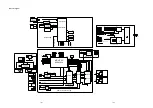
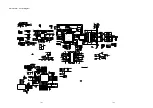
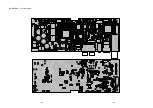
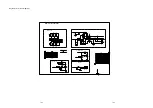
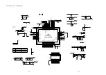
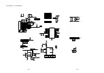
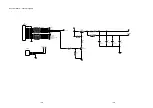
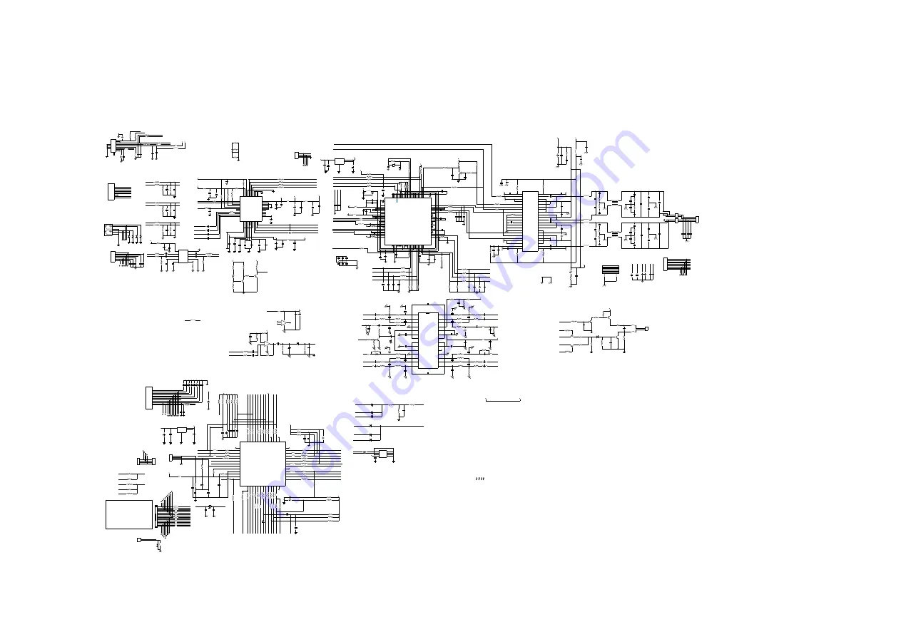
AMP Board -- Circuit Diagram

C188

100P

12-1

12-1

Summary of Contents for MCM7000/12

Page 1: ...rvicing 4 1 6 Standard Notes For Servicing Lead Free Requirements Handling Flat Pack IC 6 1 to 6 4 5 Safety Information General Notes Lead Free 7 Direction of Use 7 1 to 7 3 8 Cabinet Disassembly Instructions 8 1 to 8 2 12 AMP Board 9 Troubleshooting 9 1 to 9 2 10 Block Diagram 10 1 11 Wiring Diagram 11 1 13 Display Board 14 Headphone MP3 Link and USB LED Board Layout Diagram 12 5 15 Key Board 17 ...

Page 2: ...y Board TIPS C Component Lever Repai r M Module Lever Repair Used 55 55 58 58 61 61 79 79 93 93 94 94 96 96 98 98 51 37 12 12 05 05 Feature diffrence RDS DTS VOLTAGE SELECTOR ECO STANDBY DARK M C C C C M C C Type Versions MCM7000 Technical Specification and Connection Facilities Power Board LED Board Display Board Headphone MP3 Link Board Decoder Board AMP Board DVD Loader Key Board USB Board 1 1 ...

Page 3: ...e docking Integrated support iPad 3 MP3 Link via headphones jack from PC or MP3 player 4 Headphone Out Front of the set TBC 5 Tuner FM 6 Total output power 2x30Wrms 2 1 2 Styling Forms and Functions MCM7000 appearances are defined in their respective MUS MUS is the leading document where product appearance is applicable Features Products MCM7000 Stroke versions All Design Refer to MUS 3 for detail...

Page 4: ...k Aux In RCA cinch Tuner Socket for FM Headphone Out 3 5mm audio jack 2 1 4 Controls Local Display and LED Indications tbc Control keys on the set are MCM7000 Standby Model Source Disc USB FM Aux MP3_link Eject Play Pause Volume Rotator DSC N DBB N N N Treble Rotator Bass Rotator There is local display VFD Standby LED colour Blue in Standby mode ...

Page 5: ...y Standards Where applicable For 12 EU 05 UK 51 Russia EN IEC 60065 7 th Edition 5 6 0 0 6 L U a d a n a C S U 7 3 r o F 7 5 6 0 0 6 C E I l i z a r B 8 7 M A T A L 5 5 r o F th Edition For 98 AP 69 Singapore 75 Australia IEC 60065 7 th Edition 7 5 6 0 0 6 C E I 8 9 8 8 B G a n i h C 3 9 r o F th Edition 6 5 6 0 0 6 K a e r o K 1 6 r o F th Edition 7 5 6 0 0 6 C E I 8 0 4 4 1 S N C n a w i a T 6 9...

Page 6: ...according to UAN D1590 Ambient temperature max 40 㷄 all climates Apparatus acc to spec 5 to 35㷄 Vibration test acc IEC 60 068 2 6 operational vibration test to be proceeded in operating position of the set Level 1 2 2 4 3 4 3 4 5 4 5 4 5 7 5 7 5 7 8 Short perceptible deviations allowed Short perceptible deviations allowed Normal recallable functions functon changes allowed 3 8 10 8 10 Normal recal...

Page 7: ...Lightning Test The product shall withstand mains interference s of Differential mode 2kV 2 ohm criteria C for Europe 6kV 12 ohm criteria C for NAFTA Parameters Bi wave Open circuit voltage 2 50us Short circuit current 8 20us From 1kV to 2kV for Europe or 6kV for Nafta in steps of 1kV 10 shots per combination One shot per minute Serial impedance 2 Ohm for Europe 12Ohm for Nafta Polarity and phase P...

Page 8: ...de Performance criterion B Requirement No misoperation and no interference of user in order to guarantee continuation of performed function Reference IEC61000 4 11 For measuring method refer to UAN D1724 as far as applicable Performance criterions according to IEC61000 4 4 Amendment 1 Performance Requirement Criterion A No any degradation of specification Criterion B Temporary degradation self rec...

Page 9: ...B rated output power at 1kHz Audio Output 1 Tuner FM 67 5kHz Modulation Limit 6dB Line Out Left Right NA CD MP3 0dB track Audio Disc 1 Track 1 Headphone 15mW 2 dB RL 32 S H 0 2 e v a w e n i s z H K 1 B d 0 B S U AUX1 back 1000mV 100mV Rin 22k MP3_link front 500mV 100mV Rin 22k IPOD Docking 800mV 100mV Rin 22k Output Power 1 At THD 10 1kHz sinewave MCM7000 Main Operation for all version rms 30W 1d...

Page 10: ...5 4 0 5 m u H n o i t a l u d o M 5 4 0 5 o i t a R N S B d 4 0 e s r e v e R n o i t a c i f i l p m A 3 2 z H k 5 7 v e D q r F V m 1 F R n o i t r o t s i D Overall Frequency Response 63Hz 12 5KHz 3 dB Channel separation 400 1000 5000 Hz RF input 68 dBf 26 30 20 20 26 18 dB Frequency MHz Noise Limited Sensitivity 26 dB Image Rejection IF Rejection Large Signal Handling Selectivity S9 300 kHz FM...

Page 11: ...the pickup lens when the diode is turned on Do not look directly at the laser beam CAUTION Use of controls and adjustments or doing procedures other than those specified herein may result in hazardous radiation exposure Location Inside Top of Blu Ray mechanism Do not look directly at the laser beam coming from the pickup or allow it to strike against your skin Drive Mechanism Assembly Laser Beam R...

Page 12: ...mpartment if you are not using the product for an extended period of time Only use microfiber cloth to clean the product Important Important Safety Precautions Read and understand all instructions before you use your home theater If damage is caused by failure to follow instructions the warranty does not apply Safety Riskof electricshock or fire Never expose the product and accessories to rain or ...

Page 13: ...ic products Please act according to your local rules and do not dispose of your old products with your normal household waste Correct disposal of your old product helps to prevent potential negative consequences for the environment and human health Your product contains batteries covered by the European Directive 2006 66 EC which cannot be disposed with normal household waste Please inform yoursel...

Page 14: ... and externally exposed accessible parts RF terminals antenna terminals video and audio input and output terminals microphone jacks earphone jacks etc is lower than or equal to the specified value in the table below Measuring Method Power ON Insert load Z between B earth ground power cord plug prongs and exposed accessible parts Use an AC voltmeter to measure across the terminals of load Z See Fig...

Page 15: ...e sure that during repair you are at the same potential as the mass of the set by a wristband with resistance Keep components and tools at this same potential Available ESD protection equipment Complete kit ESD3 small tablemat wristband 4822 310 10671 Wristband tester 4822 344 13999 Be careful during measurements in the live voltage section The primary side of the power supply including the heatsi...

Page 16: ...older paste is required please contact the manufacturer of your solder equipment In general use of solder paste within workshops should be avoided because paste is not easy to store and to handle Use only adequate solder tools applicable for lead free solder alloy The solder tool must be able To reach at least a solder temperature of 400 C To stabilize the adjusted temperature at the solder tip To...

Page 17: ... this and more technical information within the magazine chapter workshop news For additional questions please contact your local repair helpdesk How to Remove Install Flat Pack IC 1 Removal With Hot Air Flat Pack IC Desoldering Machine 1 Prepare the hot air flat pack IC desoldering machine then apply hot air to the Flat Pack IC about 5 to 6 seconds Fig S 1 1 2 Remove the flat pack IC with tweezer...

Page 18: ...e flat pack IC you can remove it easily Fig S 1 3 2 Affix the wire to a workbench or solid mounting point as shown in Fig S 1 5 3 While heating the pins using a fine tip soldering iron or hot air blower pull up the wire as the solder melts so as to lift the IC leads from the CBA contact pads as shown in Fig S 1 5 4 Bottom of the flat pack IC is fixed with glue to the CBA when removing entire flat ...

Page 19: ...lectrostatic charge during unpacking or repair work 1 Ground for Human Body Be sure to wear a grounding band 1 M that is properly grounded to remove any static electricity that may be charged on the body 2 Ground for Workbench Be sure to place a conductive sheet or copper plate with proper grounding 1 M on the workbench or other surface where the semi conductors are to be placed Because the static...

Page 20: ...splay panel Display information about current source Disc compartment Hold the disc Headphone socket Switch to ECO Power or standby mode SOURCE Select a source Skip to the previous next track Skip to the previous next title or chapter Tune to a radio station Start or pause play Search backward or forward Search to a radio station Stop play Erase a program In standby mode Turn on off Demo mode 1 1 ...

Page 21: ... adjustment Mute or restore volume Start or pause play MENU Access menu This button is not workable for this model TIMER Set alarm timer Open or close the disc compartment REPEAT Select a repeat play mode Source buttons Select a source DOCK source is not available for this unit 3 Get started Caution Use of controls or adjustments or performance of procedures other than herein may result in hazardo...

Page 22: ...r connectors 2 For the left speaker identify the speaker cable that is connected to the left connectors on the main unit 3 Insert fully the red end of the speaker cable into the red connector 4 Screw the red connector to secure the cable 5 Insert fully the silver end of the speaker cable into the black connector 6 Screw the black connector to secure the cable 7 Repeat steps 2 6 for the right speak...

Page 23: ...xx CONxx Connector D3 5X12BA is specification of screw Unhook Unlock Release Unplug or Desolder e g 7 A01 seven Screws Fig D1 Fig D2 Fig NO Remove Unhook Unlock Release Unplug Desolder Note 7 A01 D3 12 BA 3 Back CAB AC Socket D3 5 A04 D3X5 PMTT 4 AMP Board D4 5 6 Power Board D5 2 A06 D3X8 PA 1 A07 D3X8 BM 1 A08 D3X5 PMTT 1 A09 D3X8 BA 1 A05 D3X8 BA Decoration Plates D6 2 A10 D3X8 FA 4 A011 D3X5 PM...

Page 24: ...8 2 Fig D3 Fig D5 Fig D4 Cabinet Disassembly Instructions A04 A04 A06 A04 A05 A09 A07 A08 Fig D6 Fig D7 Fig D8 A010 A011 A012 ...

Page 25: ... and Change the connect cable TEST Power supply voltage output CON4 each plate is normal or not 12V DC5V MCU 5V P25V replace a new one Check replace AMP MCU BOARD Replace the power board Has not voice form the speaker Check speakers boxes are connected correctly Adjust the Volume Yes Check if the operate system in MUTE state Yes Yes No Yes Retry again Cancel the MUTE setup Check replace AMP MCU bo...

Page 26: ...heck VFD display board CN401 whether connection to KEYS board CN301 is normal Check whether VFD board U401 pin 14 33 45 has V5 supply voltage and the pin 34 whether has 27V supply voltage Check pin 9 10 11 STB CLK DATA of CN401 in VFD board to see the signal is normal or not No No Check the KEYS board location B301 related electric circuit Check replace MCU board Check replace a new U401 PT6311 Te...

Page 27: ...IC DVD ON DVD RST 24C02 IR ROT A B DVD RST SP1_CS2 JUMP OPEN CLOSE FAN CON HP_MUTE HP_MUTE AUDIO_DETECT AUDIO_DETECT PHONE LINE OUT RECOUT_P1 RECOUT_P2 AC220 ECO_POWER T2 DVD 5V 2 5A T1 12V 1A 5 2V 26V 6A 150W MCU5V 1A 5V 3 5A 12V 1A AMP 5V 2 5A IPHONE 1 2 CN 2P 2 0 IPOD 5V 2 5A 4 9V 5 2V IGND MCU 5V 1 5A 4 9V 5 1V GND ECO POWER 1 2 3 4 5 6 CN 6P 2 5 12V 1A 11 7V 12 3V GND 28V 6A 28V 6A GND GND L ...

Page 28: ...RAM TS5V330CDBQR 1389G Y Pb Pr OPTICAL SPKL SPEAKER SPEAKER L SPEAKER MBOY R 2 0 2P MBOY GND SPKL SPKR SPKR HDMI FAN GND CVBS COAXIAL FFC 0 5 24P FFC 1 0 16P 2 0 5P 2 0 4P LDO 1117 1 2V LDO 1117 3 3V 7 9 2P 2 0 3P 2 0 5P MCLK BCK WCK DATA GND 2 0 6P GND 28V GND MOTOR 2 0 6P OPU 2 0 5P MOTOR TRAY IN GND TRAY OUT STBY 2 0 4P ROTA B VOLLED S3 K3 GND MCU5V PT6311 HL D1586 2 0 7P VCC D D GND 2 0 4P 2 0...

Page 29: ...33 0 R44 27 k C222 100 P R82 NC NC 0 R12 9 47 K C11 5 10 00 pF R25 10 0 FB2 FB 08 05 33R R24 1 10 K C83 15 0P C11 9 10 3 R10 3 47 R C31 68 0PF R12 3 18 K U8 R5F21 25 8 R8C 24 25 L QFP52 1 2 3 4 5 6 7 8 9 10 15 13 16 17 18 19 20 21 22 23 30 31 32 33 34 35 36 37 38 39 43 44 45 46 47 48 49 50 51 52 11 24 29 42 12 14 25 26 28 27 41 40 NC SCLK DVD_O N SSDA MODE XCIAN XCOU T RST XOU T VSS OPEN_SW M_OPEN...

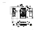
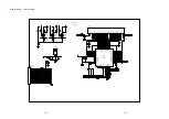
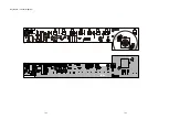
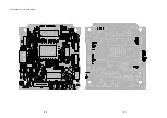
Page 30: ...AMP BOARD Layout Diagram 12 2 12 2 ...

Page 31: ...S3 6 S4 7 S5 8 S6 9 S7 10 S8 11 G1 28 G2 29 S9 12 S10 13 S11 14 S12 15 S13 16 S14 17 S15 18 S16 19 VF2 41 VF2 42 G3 30 G4 31 G5 32 G6 33 G7 34 G8 35 G9 36 G10 37 G11 38 G12 39 VFD401 HL D1586 G11 G12 Q401 NC 9014 R413 NC 10K R401 NC 4K7 R410 NC 0 R405 NC 0 V 5V S1 1 S1 Q402 NC 9014 R414 NC 10K R402 NC 4K7 R411 NC 0 R407 NC 0 V 5V S2 2 S2 Q403 NC 9014 R415 NC 10K 27V R403 NC 4K7 R412 NC 0 R409 NC 0...

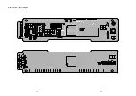
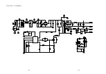
Page 32: ...Display Board Layout Diagram 12 4 12 4 ...

Page 33: ...MP3L MP3R GND L501 100uH L502 100uH L503 601 L504 601 L505 601 L506 601 1 L 2 4 3 R 5 6 7 8 9 10 11 J501 PHONE3 5 1 2 3 4 5 J502 5P MP3 L MP3 R GND 1 2 3 4 5 6 7 8 CN501 8P UGND DP DM U 5V USB BOARD 1 2 3 4 5 CN601 2 0 5P L601 601 L602 601 1GND 1 2 I O1 2 3 I O2 3 4VCC 4 U601 5V02AX 4 3 2 1 5 GND VCC DM DP UGND J601 USB GND GND UDP UDM UGND U 5V C601 104 L 5V LED LG 1 LED701 LED GUIDE BOARD WHITE ...

Page 34: ...L304 601 L305 601 L306 601 L307 601 L308 601 L309 601 L310 601 LED VOL 5V REM VFD DATA V GND VFD STB V GND VFD CLK ROT AB DIS DATA DIS STB DIS CLK 5V VF1 VF2 27V IR LED LG GND L311 601 L313 601 L314 601 L315 601 L319 601 L320 601 L321 601 L322 601 L323 601 L324 601 L325 601 L301 601 ECO K1 1 K2 1 K3 1 SK1 1 SK2 1 SK3 1 B 1 E 2 C 3 Q303 8050 D303 4148 R314 47K CE303 10UF 10V R313 4 7K R312 4 7K LED...

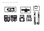
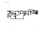
Page 35: ...Key Board Layout Diagram 12 7 12 7 ...

Page 36: ...V L5 10uH 0 6mm CE4 1500uF 25V 680uF 25V 680uF 25V R18 19 20 R21 4X120R 1206 CE5 D10 D9 CE7 1500uF 25V CE8 1000uF 25V L3 10uH 0 6mm GND GND STB C12 102 500V 1206 R30 R31 47R 1206 2 A C9 104 50V 1206 17 5V 3 5A 12V 0 5A C11 104 50V 1206 2 SF34 B CE13 220uF 16V C10 104 50V 1206 1 3 2 4 Vin Vout Gnd En C IC6 KA78L12 D5 FR157 5A 600V Q1 EL817 IC2 A C5 471 50V 0805 R16 100K 0805 C3 471 50V 0805 1 2 3 4...

Page 37: ...dc Q7 AF 9435P PIN1 2 3 PIN4 PIN5 6 7 8 Q6 C945 SOT 23 A733 SOT 23 Q5 R35 N C C15 N O C24 104 25V 1206 MC 34063 TO 6026 ZD3 6 2V 0 5W B APM4800 SOP 8 Q4 R38 10K 0805 1 2 3 4 5 6 7 8 9 9P 2 5 CON2 GND GND GND STB 17 5V 17 5V 12V 0 5A D 5V 1 5A MCU5V 20V 4A STB R32 2 0 3R 1206 G D S Power Board Circuit Diagram 2 12 9 12 9 ...

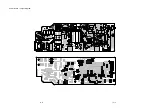
Page 38: ...T5AH 250V Power Board Layout Diagram 12 10 12 10 ...

Page 39: ...DQ13 DQ14 VSSQ DQ15 VSS C29 10nF Y1 27 000MHz U1 MX25L1605D 1 2 3 4 5 6 7 8 CS SO WP SCK HOLD SI GND VDD C3 10nF EC1 100uF 10V U3 TPS2552DBVT 1 2 3 4 5 6 IN GND ILIM EN FAULT OUT C38 10nF R68 33R C4 10nF C1 10nF C16 1nF C33 10nF FB9 MBW2012 221 R12 10K EC8 100uF 10V R27 10K U2A ZR36966 102 101 93 92 91 90 86 84 87 85 82 83 81 88 89 70 80 72 76 77 74 75 71 68 69 73 67 66 103 104 105 106 107 108 109...

Page 40: ... TP5 R38 NM 91R Q7 SS8550 1 2 3 R48 51K TP8 C52 1nF TP13 R33 0R NM TP22 Q1 BT2907 1 2 3 CN5 5P 2 0 1 2 3 4 5 LOAD LOAD OUTSW GND INSW TP4 EC9 220uF 6 3V L1 10uH R43 33R TP9 TP17 R40 2K Q2 BT2907 1 2 3 Q5 SS8550 R57 470R 1 2 3 D1 BAT54C 2 3 1 TP12 TP3 C41 NM 470pF C49 0 1uF C60 0 1uF CN3 24Pin OPU connector 24 23 22 21 20 19 18 17 16 15 14 13 12 11 10 9 8 7 6 5 4 3 2 1 25 26 27 28 GND LD DVD LD NC ...

Page 41: ...CON12 FB18 FB200 0603 FB27 FB200 0603 FB26 FB200 0603 FB19 FB200 0603 FB25 FB200 0603 R75 0R FB20 FB200 0603 FB21 FB200 0603 FB22 FB200 0603 FB23 FB200 0603 1 2 3 4 5 6 7 8 9 10 11 12 FB12 FB 0805 EC18 220uF 10V FB13 FB 0805 R66 1K C64 0 1uF Q9 AO3407 EC19 220uF 10V R65 10K CN6 5P 2 0 1 2 3 1 2 3 C65 0 1uF Q10 NNPT3904 1 2 3 Decoder Board Circuit Diagram 3 12 13 12 13 ...

Page 42: ...Decoder Board Layout Diagram 12 14 12 14 ...

Page 43: ... 12 BRACKET PLATE DURALUMIN FRONT PLATE DURALUMIN BACK PLATE S401 13 14 PCB1 VFD401 PCB2 11 100 B O T T O M P L A T E PCB4 PCB5 RUBBER FOOT RUBBER FOOT RUBBER FOOT RUBBER FOOT PCB9 PCB7 FAN1 PCB8 DVDL PCB3 13 1 13 1 ...

Page 44: ...Revision List Revision List Version 1 0 Initial Release 14 1 ...

Reviews: