CLASS 1
LASER PRODUCT
Service
Service
Service
Service
Service
MX5800SA/
21R/21S/22S/78
TABLE OF CONTENTS
Page
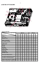
Location of pc boards & Version variations ................ 1-2
Technical Specifications ............................................. 1-3
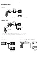
Measurement setup .................................................... 1-4
Service Aids, Safety Instruction, etc. ......................... 1-5
Disassembly Instructions & Service positions ........... 2-1
Service Test Programs ............................................... 3-1
Region codes setting, software upgrades, etc ........... 3-3
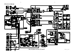
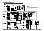
Set Block diagram & Wiring diagram ............................ 4
P-Scan board ................................................................. 5
Front Board .................................................................... 6
ECO6 Tuner Board:
System Non-Cenelec ............ 7A
System Cenelec .................... 7B
Power Module PWR207 ................................................ 8
AV Board ........................................................................ 9
5DTC Module ............................................................... 10
DAC Board ................................................................... 11
Set Mechanical Exploded view & parts list ................. 12
History .......................................................................... 13
©
Copyright 2003 Philips Consumer Electronics B.V. Eindhoven, The Netherlands
All rights reserved. No part of this publication may be reproduced, stored in a retrieval system or
transmitted, in any form or by any means, electronic, mechanical, photocopying, or otherwise
without the prior permission of Philips.
Published by KC 0333 Service Audio
Printed in The Netherlands
Subject to modification
GB
3139 785 30231
DVD Receiver
Version 1.1
MX5900SA/
37
For repair information on the SD5.00SA DVD Module, refer to Service
Manual "
DVD Module SD-5.00SA_CH - 12NC: 3122 785 13830
"
Summary of Contents for MX5800SA
Page 68: ...8239 210 93416 3139 113 3494pt6 dd wk0334 PART B 8 13 8 13 SUPPLY BOARD CHIP LAYOUT PART B ...
Page 76: ...3104 213 3525p5 dd wk0334 PART B 8 19 8 19 AMPLIFIER BOARD BOTTOM VIEW PART B ...
Page 78: ...3104 213 3525p5 dd wk0334 PART D 8 21 8 21 AMPLIFIER BOARD TOP VIEW PART D ...
Page 91: ...9 10 9 10 BOTTOM VIEW PART C PART C ...
Page 92: ...9 11 9 11 BOTTOM VIEW PART D PART D 3139 113 3500 pt6 dd wk334 ...
Page 95: ...9 14 9 14 BOTTOM VIEW PART G PART G ...
Page 96: ...9 15 9 15 BOTTOM VIEW PART H PART H 3139 113 3500 pt6 dd wk334 ...
Page 104: ...10 5 10 5 Exploded view 5DTC mechanic for orientation only ...
Page 111: ...BOTTOM VIEW COMPONENT LAYOUT For pcb layout 35037 11 4a 11 4a 3139 113 3503 pt 7 dd wk414 ...
Page 112: ...TOP VIEW PART A 11 5 11 5 PART A ...
Page 113: ...TOP VIEW PART B 11 6 11 6 PART B ...
Page 115: ...TOP VIEW PART B For pcb layout 35037 11 6a 11 6a 3139 113 3503 pt 7 dd wk414 PART B ...
Page 126: ...12 1 12 1 EXPLODED VIEW MAIN UNIT MX5800SA exploded view 3139 119 35170 dd wk318 ...


