8-2
8-2
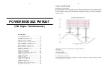
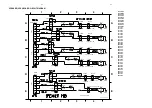
Block diagram and operation
clock
generator
output 1
output 2
output 3
output 4
output 5
output 6
input 1
input 2
input 3
input 4
input 5
input 6
freq_hop
301.35 / 350 kHz
DC
detection
err
temp
NTC
TDA8920
TDA8920
TDA8920
output 1
input 1
TDA8920
SINGLE ENDED 6 x 75W
BRIDGE 3 x 100W
+
-
input 2
TDA8920
+
-
input 3
TDA8920
+
-
clock
generator
freq_hop
301.35 / 350 kHz
DC
detection
err
temp
NTC
output 2
output 3
• clock oscillator
The clock frequency is generated around IC7600. Using 2 extra transistors (7602 and 7608) and 2 ceramic resonators it can be operated at
2 frequencies: 602.7kHz and 700kHz. The frequency is selected by the signal “FREQ_HOP” coming from connector 1301 pin 9.
When FREQ_HOP is low, the output of 7600-1 will be high. This switches transistor 7602 on, and connects resonator 1600 (602.7kHz) to inverter
7600-3. Similarly, when FREQ_HOP is high, resonator 1601 is connected to 7600-3.
The output frequency is divided by two by IC7607, resulting in 301.35kHz or 350kHz.
The purpose of a selectable clock frequency is related to the disturbance of the tuner which is built-in together with this amplifier. In MW, the
software of the set microprocessor will select the other clock frequency in case the amplifier clock interferes with the tuned station.
• Class-D amplifier TDA8920 and low-pass filter
The TDA8920 is a two channel audio power amplifier using class-D technology. The audio input signal is converted into a digital Pulse Width
Modulated (PWM) signal via an analog input stage and PWM modulator. It is then fed to the power stage which outputs a high power PWM
signal which switches between the main supply lines.
The TDA8920 is followed by a 2nd-order low-pass filter. It has a cut-off frequency around 50kHz and converts the PWM signal into analog audio
signal across the loudspeaker.
The TDA8920 has a temperature protection and a current limiter built-in.
Furthermore, the IC can be put in active, mute and standby mode.
- Active mode (amplifier fully operational) with output signal.
- Mute mode; the amplifiers are operational, but the audio is muted
- Standby mode; with a very low supply current, the output stage is switched off.
• DC-detection
The DC-detection circuit monitors all 6 outputs for DC. Whenever one or more outputs contain DC for more than 1 second, the circuit will be
activated. A positive voltage will activate transistor 7710 and pin 10 of connector 1301 will be pulled down. In case of a negative voltage, transistor
7716 will be activated, which in turn activates 7710. The set microprocessor will take further action.
3104 217 07180 bl110
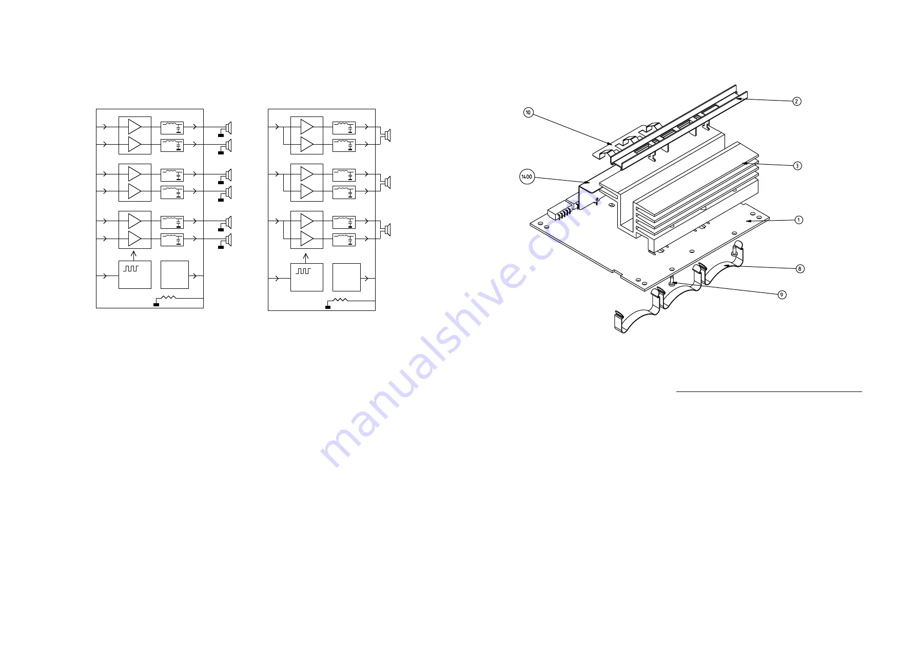
MECHANICAL EXPLODED VIEW
MECHANICAL PARTS LIST & SCREWS
8
3104 211 29861
SPRING 6 CHANNEL
9
-
D2.3 x 8
10
3104 211 29881
EARTH SPRING
Note:
Only the parts mentioned in this list are normal service
spare parts.
Summary of Contents for MX5800SA
Page 68: ...8239 210 93416 3139 113 3494pt6 dd wk0334 PART B 8 13 8 13 SUPPLY BOARD CHIP LAYOUT PART B ...
Page 76: ...3104 213 3525p5 dd wk0334 PART B 8 19 8 19 AMPLIFIER BOARD BOTTOM VIEW PART B ...
Page 78: ...3104 213 3525p5 dd wk0334 PART D 8 21 8 21 AMPLIFIER BOARD TOP VIEW PART D ...
Page 91: ...9 10 9 10 BOTTOM VIEW PART C PART C ...
Page 92: ...9 11 9 11 BOTTOM VIEW PART D PART D 3139 113 3500 pt6 dd wk334 ...
Page 95: ...9 14 9 14 BOTTOM VIEW PART G PART G ...
Page 96: ...9 15 9 15 BOTTOM VIEW PART H PART H 3139 113 3500 pt6 dd wk334 ...
Page 104: ...10 5 10 5 Exploded view 5DTC mechanic for orientation only ...
Page 111: ...BOTTOM VIEW COMPONENT LAYOUT For pcb layout 35037 11 4a 11 4a 3139 113 3503 pt 7 dd wk414 ...
Page 112: ...TOP VIEW PART A 11 5 11 5 PART A ...
Page 113: ...TOP VIEW PART B 11 6 11 6 PART B ...
Page 115: ...TOP VIEW PART B For pcb layout 35037 11 6a 11 6a 3139 113 3503 pt 7 dd wk414 PART B ...
Page 126: ...12 1 12 1 EXPLODED VIEW MAIN UNIT MX5800SA exploded view 3139 119 35170 dd wk318 ...


