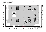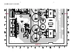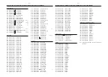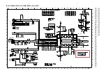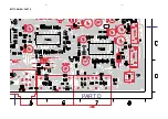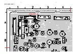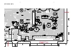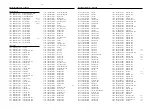
BRIEF INTRODUCTION OF THE AV BOARD
The AV Board consists of the following features :
a.
IC 7130 (TDA7468D)
IC 7130 provides the source selection (TUNER, TV/AV Digital in, DVD/CD & AUX) and basic sound processing - bass, treble, volume
& mute controls for the Front L/R loudspeakers.
Note: Although provided for, the AUX source (pin 3 and 26) are never selected & instead and additional IC 7422 (HEF4052BT) is used
to include a TV in from the Scart connector socket.
Sound features are controlled by the microprocessor IC on the Front Board via I
2
C Bus.
Undesirable noise during source switching are muted off via the software of the microprocessor IC on the Front Board.
b.
IC 7422 (HEF4052BT)
This IC allows the additon of another TV source via the SCART connector socket. The output MUX_L/MUX_R will go to pin 4 and 25
of IC 7130.
c.
Line out mute
Line out mute is done via the transistors 7100, 7132, 7133 and 7150 during Power up/down, Source and sound switching (MUTE-LO,
active low) and Disc & Digital in modes (MUTE_AV, active high).
d.
Headphone amplifier / pre-amplifier
IC 7230 (NJM4556AM) is used as headphone amplifer and pre-amplification for the Front L/R signal to the Amplifier board. The
transistors matrix 7200, 7231, 7232, 7233 and 7250 allows the heaphone out to be muted when inserting the headphone
e.
IC 7304 and 7330 (TDA7468D)
IC 7304 and 7330 provides creation of matrix sound (via Line-L/R from IC 7130) during non-DVD source and sound processing - bass,
treble, volume & mute controls for the Center/Subwoofer and Surround L/R loudspeakers respectively.
Sound features are controlled by the microprocessor IC on the Front Board via I
2
C Bus.
Undesirable noise during source switching are muted off via the software of the microprocessor IC on the Front Board.
f.
IC 7352 (74HC4051D)
This multiplexer output (MUX_DET) informs the microprocess IC on the Front Board on the type of connection & condition the set is in.
g.
IC 7402 (M62320FP)
The IC serves as I
2
C Expander to provide for additional control lines required.
AV BOARD
TABLE OF CONTENTS
Brief Introduction of the AV Board ............................................ 9-1
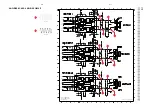
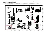
Inputs, Source Sel. & Vol cont. L/R Circuit .............................. 9-2
HP amp / Pre-amp., Supply & Interconnection Circuit ............ 9-3
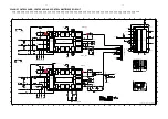
Volume cont. Surr L/R, Cen & SW & Multiplexer Circuit ......... 9-4
Digital in/out, S-video, Scart, & I
2
C Expander Circuit .............. 9-5
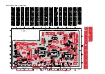
Bottom view - Chip & Discrete layouts (Part A to D) ............... 9-6
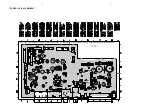
Top view - Component & Chip layouts (Part E to H) ............... 9-7
Bottom view Part A ................................................................... 9-8
Bottom view Part B ................................................................... 9-9
Bottom view Part C ................................................................. 9-10
Bottom view Part D ................................................................. 9-11
Top view Part E ....................................................................... 9-12
Top view Part F ....................................................................... 9-13
Top view Part G ...................................................................... 9-14
Top view Part H ...................................................................... 9-15
Electrical parts list .................................................................. 9-16
9-1
9-1
Summary of Contents for MX5800SA
Page 68: ...8239 210 93416 3139 113 3494pt6 dd wk0334 PART B 8 13 8 13 SUPPLY BOARD CHIP LAYOUT PART B ...
Page 76: ...3104 213 3525p5 dd wk0334 PART B 8 19 8 19 AMPLIFIER BOARD BOTTOM VIEW PART B ...
Page 78: ...3104 213 3525p5 dd wk0334 PART D 8 21 8 21 AMPLIFIER BOARD TOP VIEW PART D ...
Page 91: ...9 10 9 10 BOTTOM VIEW PART C PART C ...
Page 92: ...9 11 9 11 BOTTOM VIEW PART D PART D 3139 113 3500 pt6 dd wk334 ...
Page 95: ...9 14 9 14 BOTTOM VIEW PART G PART G ...
Page 96: ...9 15 9 15 BOTTOM VIEW PART H PART H 3139 113 3500 pt6 dd wk334 ...
Page 104: ...10 5 10 5 Exploded view 5DTC mechanic for orientation only ...
Page 111: ...BOTTOM VIEW COMPONENT LAYOUT For pcb layout 35037 11 4a 11 4a 3139 113 3503 pt 7 dd wk414 ...
Page 112: ...TOP VIEW PART A 11 5 11 5 PART A ...
Page 113: ...TOP VIEW PART B 11 6 11 6 PART B ...
Page 115: ...TOP VIEW PART B For pcb layout 35037 11 6a 11 6a 3139 113 3503 pt 7 dd wk414 PART B ...
Page 126: ...12 1 12 1 EXPLODED VIEW MAIN UNIT MX5800SA exploded view 3139 119 35170 dd wk318 ...


