13-1
DOCUMENT HISTORY
Version 1.0
*
Initial release
Version 1.1
*
Add MX5800SA/78 into the Service Manual and some correction
Pages modified:
Pg Front, 1-1, 1-2 and 3-3 and 12-2
Pages corrected:
Pg 6-16, 8-2, 12-3 (added)
*
Add new pcb layout & schematics released
Power Module:
Pg 8-3a to 8-13a
DAC Board:
Pg 11-3a to 11-10a
Summary of Contents for MX5800SA
Page 68: ...8239 210 93416 3139 113 3494pt6 dd wk0334 PART B 8 13 8 13 SUPPLY BOARD CHIP LAYOUT PART B ...
Page 76: ...3104 213 3525p5 dd wk0334 PART B 8 19 8 19 AMPLIFIER BOARD BOTTOM VIEW PART B ...
Page 78: ...3104 213 3525p5 dd wk0334 PART D 8 21 8 21 AMPLIFIER BOARD TOP VIEW PART D ...
Page 91: ...9 10 9 10 BOTTOM VIEW PART C PART C ...
Page 92: ...9 11 9 11 BOTTOM VIEW PART D PART D 3139 113 3500 pt6 dd wk334 ...
Page 95: ...9 14 9 14 BOTTOM VIEW PART G PART G ...
Page 96: ...9 15 9 15 BOTTOM VIEW PART H PART H 3139 113 3500 pt6 dd wk334 ...
Page 104: ...10 5 10 5 Exploded view 5DTC mechanic for orientation only ...
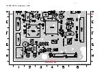
Page 111: ...BOTTOM VIEW COMPONENT LAYOUT For pcb layout 35037 11 4a 11 4a 3139 113 3503 pt 7 dd wk414 ...
Page 112: ...TOP VIEW PART A 11 5 11 5 PART A ...
Page 113: ...TOP VIEW PART B 11 6 11 6 PART B ...
Page 115: ...TOP VIEW PART B For pcb layout 35037 11 6a 11 6a 3139 113 3503 pt 7 dd wk414 PART B ...
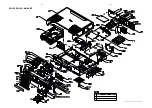
Page 126: ...12 1 12 1 EXPLODED VIEW MAIN UNIT MX5800SA exploded view 3139 119 35170 dd wk318 ...

