background image

This assemby drawing shows a summary of all possible versions.  For components used in a specific version
see schematic and respective parts list.

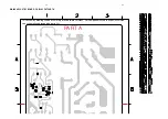
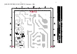
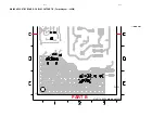
PART A

8-12

8-12

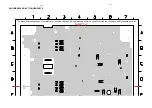
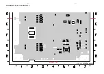
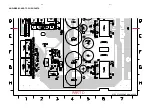
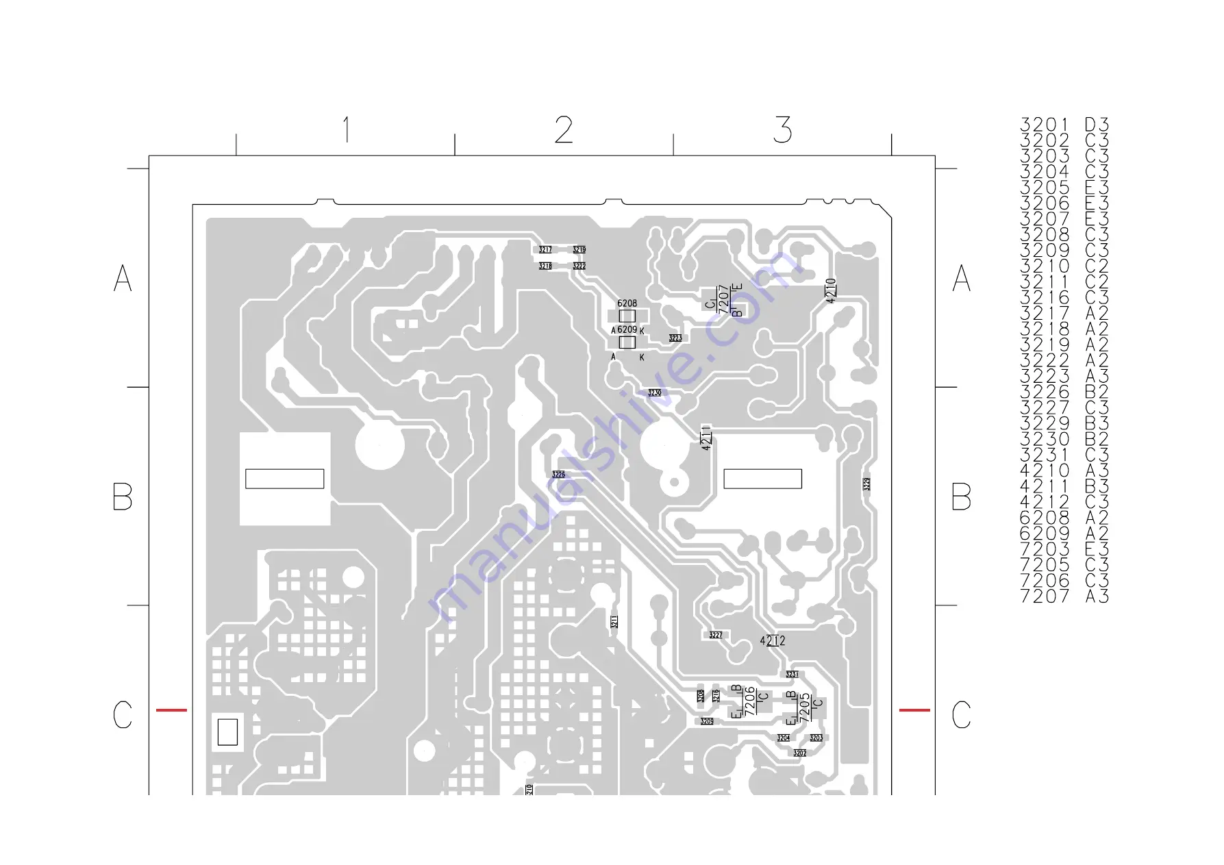
SUPPLY BOARD - CHIP LAYOUT PART A

Summary of Contents for MX5800SA

Page 1: ...em Cenelec 7B Power Module PWR207 8 AV Board 9 5DTC Module 10 DAC Board 11 Set Mechanical Exploded view parts list 12 History 13 Copyright 2003 Philips Consumer Electronics B V Eindhoven The Netherlands All rights reserved No part of this publication may be reproduced stored in a retrieval system or transmitted in any form or by any means electronic mechanical photocopying or otherwise without the...

Page 2: ...t x x x x x x S Video Output x x x x x x Headphone Socket x x x x x x P Scan board Faroudja P scan x Tuner board ECO6 System non Cenelec x x x x x Tuner board ECO6 System Cenelec x 75W 6 Ch Single SW with 1x Amplifier pcb 75W 7 Ch Twin SW with 1x Amplifier pcb x x x x x x VERSION VARIATIONS Type Versions MX5800SA MX5800SA Features Board in used MAIN AMPLIFER 75W MAINS BOARD 5DTC DVD LOADER MECHANI...

Page 3: ...ode 3 75W RMS channel Frequency response 3dB 20Hz 20kHz Hum minimum volume 200nW Residue noise min volume 40nW Digital Sound Control Stereo 3D Sound Multi modes 4 Bass Treble 3 to 3 4 Input sensitivity TV in 350mV 3dB Aux in 880mV 2dB Output sensitivity Line out 600mV 2dB at 47kΩ Headphone vol max 660mV 2dB at 32Ω COMPACT DISC VCD DVD Video Decoding MPEG 2 MPEG 1 Video DAC 10 Bits Signal System PA...

Page 4: ...z e g 7122 707 48001 LF Voltmeter e g PM2534 DUT S N and distortion meter e g Sound Technology ST1700B Frame aerial e g 7122 707 89001 Tuner AM MW LW To avoid atmospheric interference all AM measurements have to be carried out in a Faraday s cage Use a bandpass filter or at least a high pass filter with 250Hz to eliminate hum 50Hz 100Hz RF Generator e g PM5326 Ri 50Ω Bandpass 250Hz 15kHz e g 7122 ...

Page 5: ...97 30245 CD RW Printed Audio Test Disc 7104 099 96611 Dolby Pro logic Test Disc 4822 395 10216 ESD Equipment Anti static table mat large 1200x650x1 25mm 4822 466 10953 Anti static table mat small 600x650x1 25mm 4822 466 10958 Anti static wristband 4822 395 10223 Connector box 1MΩ 4822 320 11307 Extension cable to connect wristband to conn box 4822 320 11305 Connecting cable to connect table mat to...

Page 6: ...n osservazione della più grande cauzione alla loro manipolazione Durante le riparazioni occorre quindi essere collegato allo stesso potenziale che quello della massa dell apparecchio tramite un braccialetto a resistenza Assicurarsi che i componenti e anche gli utensili con quali si lavora siano anche a questo potenziale Pour votre sécurité ces documents doivent être utilisés par des spécia listes ...

Page 7: ...sed Figure 2 1 Loosen 3 screws D and 2 catches C2 on the Rear panel pos 251 to remove theTuner board assemby pos 1101 as pe figure 3 2 Loosen 1 screws E and 2 catches C3 to unslot the Mains board pos 1102 A out of the Rear panel as per figure 4 3 Loosen bracket pos 254 by turning a catch sliding towards the outside and lifting it upwards as per figure 5 4 Loosen 8 screws F 7 screws for non Scart v...

Page 8: ... pos 1103 B as per figure 7 4 Loosen 2 screws K and 2 catches C7 to remove the P Scan board pos 1107 as per figure 7 applicable for MX5900SA only 5 Loosen 2 screws H to remove the bracket pos 260 as per figure 8 6 Loosen 3 screws L to remove the SACD SD 5 0SA_CH board pos 1103 C as per figure 9 7 Loosen 3 screws G lift up the 5DTC Module s pos 1103 A rear and pull the module out towards the rear a...

Page 9: ...ault finding on other parts of the set 3 Insulation sheet eg thick paper or cardboard should be use during fault finding to prevent short circuiting of copper patterns to metallic surroundings Service positions 2 3 2 3 Thick paper Thick paper or insulation sheet shouldbeusedtopreventpcboards copper tracks from short circuiting to bottom plate Mains Board with non conductive insulation attached to ...

Page 10: ...r than 69 the set goes into Standby Return the value assign for the different possible options CLOCK TIMER Button pressed Y Y Y N N N CLOCK TIMER Button pressed 9 Button pressed Display shows 32K Output at Front Board pin 19 of uP 2048Hz Display shows 12M Output at Front Board pin 19 of uP 2 929 6875Hz QUARTZ TEST TUNING Button pressed Disconnect Mains cord Y Y N N Y Display Tuner Version ccc Serv...

Page 11: ...t successful Radial test is started Press BII if test is successful and PROGRAM button if test is not successful The laser spot jumps to another position Press BII to jump to the next position or press PROGRAM to jump to previous position Reads out the info from the error log Up to 16 errors 8 hex digits can be stored in a buffer Press BII to view next error or press PROGRAM to view previous error...

Page 12: ...n is confidential and may not be distributed Only a qualified service person should reprogram the mono BE board After replacement repair of the Mono BE board the customer settings and also the region code may be lost Reprogramming will put the set back in the state in which it has left the factory i e with the default settings and the allowed region code Reprogramming will be done by way of the Re...

Page 13: ...A8920 LPS COIL MAINS TRAFO SURROUND 1 2XTDA8920 TDA8920 L R TDA8920 POWER AMP DVD Module Power Amplifier Front Display POWER AMP Mains and Regulator ECO 6 TMP88CU74F ECO Standby MX3900D_130_wk302 2 Note All others are in the AV board ...

Page 14: ... Prefold CVBS FRONT DISPLAY 16P 18P K ok 180mm MX39 55 56 4P MX39 55 56 59 for MX3900D K ok Prefold Prefold AD Prefold AD for MX5500 5600 DVD_R 340mm 4P 220mm MX39 55 56 2P FE 1 AD Prefold 240mm DVD_Ls GND_S DVD_C POWER SWITCH MX5800SA DPL2_L TUNER 10P 10P 5P AD 120mm 400mm 17P MIC_IN DVD_L 1 AD AD 180mm FMN GND_d 1 GND_V Y_G_Y 10 13P DPL2_R SCART 0 13P 14P 220mm MX58 100mm 7P 1 DIG_IN_1 22P 220mm...

Page 15: ... 120mm EH 4P 120mm EH 4P 120mm EH 4P SPK I EH 4P 220mm EH 5P 10P Prefold BD 120mm EH 9P 120mm 1 120mm EH 8P 140mm EH 5P 180mm 1 100W 5 6 7 8 9 3104 213 3525 75W EH 8P R L CENTER SUR R Amplifier 1 1 1 3104 213 3525 1 NOTE 75W 6 CHANNEL 1 X CLASS D AMPLIFIER SPK I 75W 7 CHANNEL 1 X CLASS D AMPLIFIER SPK I SPK II 100W 2 X CLASS D AMPLIFIER SPK I SPK II EH 240mm 4P Blue Yellow 1 Red Black SUPPLY 1 TRA...

Page 16: ...V GND ODD EVEN WORK_CLK SEL_DSD GND BIT_CLK DSD_CLK GND 256FS GND SCL DAC SDA DAC GND DSD_PCM8 NC SCL DAC DSD_PCM9 NC INT_REQ DAC_RST CLK_SEL I2C_DATA_DVD SCART1 B_REF G_REF G_Y YC3 5V Y_REF Y C_REF C CVBS_REF CVBS B_U SCART0 3V3 3V3 DSD_PCM9 P50 GPIO2 NC GPIO3 GPIO1 NC 3V3 3V3 5V 12V GND PCMSCLK NC SACHI 5 0 GND PCMCLK NC PCMLRCLK GND SPDIF MUTE 12V I2C_CLK_DVD GND 27MHZ CLK GND DSD_LFE GND DSD_C...

Page 17: ...TECHNICAL REMARKS P SCAN BOARD TABLE OF CONTENTS Top View Layout 5 2 Bottom View Layout 5 3 Circuit Diagram Part 1 5 4 Circuit Diagram Part 2 5 5 Electrical parts list 5 6 5 1 5 1 ...

Page 18: ...P SCAN BOARD TOP VIEW LAYOUT This assembly drawing shows a summary of all possible versions For components used in a specific version see schematic diagram and respective parts list 3139 113 3516 pt2 dd wk0315 ...

Page 19: ... SCAN BOARD BOTTOM VIEW LAYOUT This assembly drawing shows a summary of all possible versions For components used in a specific version see schematic diagram and respective parts list 3139 113 3516 pt2 dd wk0315 ...

Page 20: ... R Cr CrCb_5 38 R Cr CrCb_6 39 R Cr CrCb_7 40 R V PR_OUT_2 140 141 R V PR_OUT_3 R V PR_OUT_4 142 R V PR_OUT_5 143 144 R V PR_OUT_6 R V PR_OUT_7 145 SCLK 45 SDATA 46 SDRAM_ADDR0 103 SDRAM_ADDR1 102 SDRAM_ADDR10 91 SDRAM_ADDR2 101 SDRAM_ADDR3 100 HSYNC2_PORT1 5 HSYNC_PORT2 208 4 IN_CLK1_PORT1 IN_CLK2_PORT1 10 IN_SEL 41 OE 156 PLL_PVDD 157 PLL_PVSS 158 RESET_N 47 R Cr CrCb_0 29 32 R Cr CrCb_1 R Cr Cr...

Page 21: ...3V3_SCAN 100p 2421 10u GND_PS 3 2 7 5 6 1 4 14 7203 A 74LVT86DB 2216 100n 3V3D_V 12 13 11 14 7 4201 3V3D_V 7200 A 74LVT74DB 100n 2413 1u5 5420 4u7 150p 2420 5421 100n 2403 3402 150R 1K2 3414 100n 2218 3415 1K2 150p 2400 3416 75R 100p 2401 GND_PS 150R 3401 150R 3403 1K2 3405 3404 1K2 75R 3406 5V_P_SCAN 3V3D 3422 150R 3421 150R 150R 3423 1K2 3425 3424 1K2 4 1 5 2 75R 3426 5401 1u5 7400 AD8061 3 3 4 ...

Page 22: ...22R 5 0 062W 3107 4822 051 30101 100R 5 0 062W 3108 4822 051 30101 100R 5 0 062W 3109 4822 117 12139 22R 5 0 062W 3110 4822 117 12139 22R 5 0 062W 3111 4822 117 12139 22R 5 0 062W 3112 4822 117 12139 22R 5 0 062W 3113 4822 117 12139 22R 5 0 062W 3114 4822 117 12139 22R 5 0 062W 3115 4822 117 12139 22R 5 0 062W 3116 4822 117 12139 22R 5 0 062W 3117 4822 117 12139 22R 5 0 062W 3118 4822 117 12139 22...

Page 23: ...in No 1 2 3 4 5 6 7 8 9 10 11 12 13 14 15 16 17 18 19 Symbol VDD VSS CS1 RES A0 RD WR D0 D1 D2 D3 D4 D5 D6 D7 LED LED BZ1 BZ2 Description Power supply for logic circuit 5V Ground 0V Input when CS1 0 the chip select become active Input low active System reset Usually connected to the low order bit of the MPU address bus and used to identify the data or a command A0 1 D0 D7 are display data A0 0 D0 ...

Page 24: ...tion input with pull high resistor When the CS is logic high the data and command read from or written to the HT1621 are disabled The serial interface circuit is also reset But if CS is at logic low level and is input to the CS pad the data and command transmission between the host controller and the HT1621 are all enabled READ clock input with pull high resistor Data in the RAM of the HT1621 are ...

Page 25: ...ble versions For components used in a specific version see schematic and respective parts list 8239 210 9413 pt4 dd wk0323 This assemby drawing shows a summary of all possible versions For components used in a specific version see schematic and respective parts list 8239 210 9413 pt4 dd wk0323 ...

Page 26: ... 6119 D10 7103 F7 7104 G6 7105 H4 7106 C2 7107 C3 7109 A9 7111 B7 7112 B8 6119 1N4003 10K 3117 1K0 2111 1u0 E0 1 E1 M24C02 7103 2117 4554 x x x x x 4556 x 5800 4550 5K6 Provision 5900 4551 4552 3174 120R 3175 120R 68R 68R 3191 3174 3190 1K 4K7 3141 3144 3143 4K7 3180 10K 4K7 10K 3181 3182 10K 4K7 3142 RT 01T 1905 1906 RT 01T 7109 BC847B 3194 1K0 4555 10K 3175 3201 3200 10K 1K0 1K0 3196 1K0 3197 1K...

Page 27: ...ersions For components used in a specific version see schematic and respective parts list 8239 210 9501 pt5 dd wk0334 Part A Part B This assemby drawing shows a summary of all possible versions For components used in a specific version see schematic and respective parts list 8239 210 9501 pt5 dd wk0334 ...

Page 28: ...6 6 6 6 FRONT DISPLAY PART CHIPS LAYOUT PART A Part A This assemby drawing shows a summary of all possible versions For components used in a specific version ...

Page 29: ...6 7 6 7 FRONT DISPLAY PART CHIPS LAYOUT PART B Part B fic version see schematic and respective parts list 8239 210 9501 pt5 dd wk0334 ...

Page 30: ...01 B1 T502 B1 T503 B1 T504 C1 T505 C1 3502 120R Standby 1501 FE ST VK N 1500 1 2 3 4 6501 LTL 816GE 2501 GND_B 2u2 10K 100R 3503 3504 470R 3501 GND_B 6500 LTL 816EELC BC847B 7504 7500 BC847B 3506 470R 3505 470R 100p GND_B 5 OUT 1 VS 3 2502 7501 TSOP4836ZC1 GND GND 2 4 C C RC6 Stdby_key C C Stdby_LED LPS_LED 8239 210 9414 pt4 dd wk0323 POWER SWITCH PART CIRCUIT DIAGRAM ...

Page 31: ...specific version see schematic and respective parts list 8239 210 9414 pt4 dd wk0323 This assemby drawing shows a summary of all possible versions For components used in a specific version see schematic and respective parts list 8239 210 9414 pt4 dd wk0323 POWER SWITCH PART COMPONENT CHIPS LAYOUT ...

Page 32: ...5 7602 B5 agnd 1605 5605 RK09D mic_gnd 3612 20K 2610 680p 5606 4 6 1 2 5 47n 2612 agnd agnd YKB21 5005G 1600 1 2 3 4 5 7 8 10K 3613 mic_gnd 5600 agnd RT 01T 1604 1 1u0 2605 22n 2600 10K 3610 3609 1M0 2 3 4 5 6 7 8 7601 BC847B mic_gnd 1602 FE ST VK N 1 5608 5609 1n0 2607 1M0 3608 4604 1606 1 22n 2602 agnd 2606 47n mic_gnd 47n 2611 3606 agnd 5607 2K7 2609 47n 2 4 5 3 1 100u 2603 2615 47n 2604 1u0 56...

Page 33: ...sible versions For components used in a specific version see schematic and respective parts list 8239 210 9415 pt6 dd wk0334 This assemby drawing shows a summary of all possible versions For components used in a specific version see schematic and respective parts list 8239 210 9415 pt6 dd wk0334 ...

Page 34: ... 12 FRONT CONTROL PART CHIPS LAYOUT This assemby drawing shows a summary of all possible versions For components used in a specific version see schematic and respective parts list 8239 210 9412 pt5 dd wk0334 ...

Page 35: ...3 This assemby drawing shows a summary of all possible versions For components used in a specific version see schematic and respective parts list 8239 210 9412 pt5 dd wk0334 FRONT CONTROL PART COMPONENT LAYOUT ...

Page 36: ...13 12 11 9 10 1 16 8 7303 74HC4094D 3 2 15 4 5 6 7 14 GND_B 7300 120R 3339 6305 1304 LTL 816TDK3 3352 7301 BC847B 120R 7308 BC847B 2K7 3311 3355 10K 10K 3354 CLK 1307 GND_B BC847B 7304 1309 PROGRAM 3303 GND_B GND_B 120R 3343 120R 3341 1K8 3310 3306 390R 3305 270R SWEETSPOT 1301 47p 2309 2305 120R 3349 10n NEXT 1305 GND_B LTL 816TDK3 6303 LTL 816TDK3 6302 3309 1K2 3332 1303 GND_B STOP 16 2 3 4 5 6 ...

Page 37: ...22 051 30103 10k 5 0 062W RDS 3108 4822 051 30152 1k5 5 0 062W RDS 3109 4822 051 30102 1k 5 0 062W RDS 3110 4822 051 30103 10k 5 0 062W non RDS 3111 4822 051 30102 1k 5 0 062W RDS 3112 4822 051 30103 10k 5 0 062W non RDS 3113 4822 117 12891 220k 1 ERJ3E RDS 3114 4822 051 30222 2k2 5 0 062W RDS 3115 4822 051 30103 10k 5 0 062W 3116 4822 051 30103 10k 5 0 062W 3117 4822 051 30102 1k 5 0 062W 3118 48...

Page 38: ...0008 0R Jumper 0603 4248 4822 051 30008 0R Jumper 0603 4256 4822 051 30008 0R Jumper 0603 4257 4822 051 30008 0R Jumper 0603 4301 4822 051 30008 0R Jumper 0603 4302 4822 051 30008 0R Jumper 0603 22S 4303 4822 051 30008 0R Jumper 0603 22S 4304 4822 051 30008 0R Jumper 0603 4305 4822 051 30008 0R Jumper 0603 22S 4306 4822 051 30008 0R Jumper 0603 4307 4822 051 30008 0R Jumper 0603 4309 4822 051 3000...

Page 39: ... 6 5 43 C D 450kHz 450kHz 450kHz 20 75kHz VStabA VStabB VStabB VStabA VStabB 10 7 MHz 10 7 MHz 35 9 Vdd Vcc1 7 23 VStabA VStabB 38 34 22 Vcc2 8 ECO6 Systems 140499 LF filter RDS MPX RDS MPX stereo clock data enable Version 1120 1 8 FM Frontend AM Frontend AM FRAME AERIAL B 1103 1101 1102 A FM MPX buffer ampl 5 Discriminator 10 7 MHz Vdd Vcc1 Vcc Vcc2 AM RF AM Osc FM Osc FM RF FM IF 1 FM IF 2 AM IF...

Page 40: ...1n 3134 22K 6105 2 HN1V02H 100n 2163 T141 7KL 1K 3144 5102 3157 100K T109 470R 3153 2130 22n 220R 3105 3142 100K 3167 120R 33p 2149 2K2 3145 1132 C PAD T103 T111 2164 470n T102 2140 15p 2139 2138 2u2 82p 2133 1u 3103 8K2 T120 4p7 2154 3156 1101USA YKD21 100K 2161 100n 5119 2119 10p T142 5123 11p 2106 3172 6106 BAS216 100n 2165 5K6 3154 3155 220R 330R 2124 33K 3176 22n WRITE EN 5114 7P MUTE P0 P1 P...

Page 41: ...riginal frame antenna has to be used 2 RC network serves for damping the IF filter while adjusting the other one 4 MW has to be aligned before LW Waverange Input frequency Input Tuned to Adjust Output Scope Voltmeter FM 87 5 108MHz 65 81 74 87 5 108MHz FM MW version 9kHz grid 531 1602kHz as low as possible ECO6 System non Cenelec stage 3 120900 TUNER BOARD ECO6 Systems non Cenelec componentside vi...

Page 42: ...10 63V RDS only RESISTORS 3101 4822 051 20333 33kΩ 5 0 1W 3102 4822 117 10837 100kΩ 1 0 1W 3103 4822 051 20822 8 2kΩ 5 0 1W 3104 4822 117 13577 330Ω 1 0 1W 3105 4822 117 11503 220Ω 5 0 1W 3132 4822 051 20479 47Ω 5 0 1W 3134 4822 051 20223 22kΩ 5 0 1W 3141 4822 117 11148 56kΩ 1 0 1W 3142 4822 100 12159 TRIMPOT 100kΩ RESISTORS 3143 4822 051 20223 22kΩ 5 0 1W RDS only 3144 4822 051 10102 1kΩ 2 0 25W ...

Page 43: ... B V Stab B V Stab A V Stab B 10 7 MHz 10 7 MHz 35 9 Vdd Vcc1 7 23 V Stab A V Stab B 38 34 22 Vcc2 8 ECO6 Systems Cenelec 140499 V Loop FM AM RF AM Osc FM IF 1 FM IF 2 LF filter MPX buffer ampl RDS MPX 5 RDS MPX stereo clock data enable Version 3 1120 AM IF 1 AM IF 2 AM AFC 1 8 AM Frontend 2 AM FRAME AERIAL B 1103 1101 1102 A FM AM FM Discriminator 10 7 MHz Vdd FM Vcc1 Vcc Vcc2 MW LW AM RF AM Osc ...

Page 44: ...4 22n USA 22n USA C PAD 1131 T141 2106 11p 20p_LW 0R 4104 0R 41xx 2165 100n 1130 C PAD 10K 3180 2150 100n BZX284 C11 6107 T102 2127 220n 2169 2n2 100K 3170 1 I 3 O 2125 560p 5109 2 G 470R 3152 2108 100p 3125 10K 3153 470R 330R 3193 T103 120R 3167 100R 3195 7 8 33K 3176 8 5122 1 2 3 4 6 5123 1 2 3 4 6 7 5110 G 2 I 1 O 3 5115 1 2 3 4 6 7 8 2 3 4 6 7 8 5119 1 2135 100n 2163 LW 7104 BC337 40 2145 220p...

Page 45: ...ce Testprogram By selecting the TUNER TEST test frequencies will be stored as preset frequencies automatically AM FRAME AERIAL FM 75Ω FM FRONTEND Birdy Filter ECO6 Sys Cenelec layout stage 6 160501 1101 B5 1102 B5 1103 C5 1110 B4 1120 A4 1130 A5 1131 C5 1132 A4 2106 B4 2107 B3 2128 A3 2129 B3 2133 C1 2138 B1 2144 B1 2162 A4 2191 B4 3142 C2 5102 C4 5103 C4 5109 B3 5110 A2 5111 A3 5112 A2 5114 A2 51...

Page 46: ...98 021 38210 820Ω 5 0 06W 3132 4822 051 20479 47Ω 5 0 1W 3134 4822 051 20223 22kΩ 5 0 1W 3135 3198 021 31020 1kΩ 5 0 06W 3137 4822 051 20223 22kΩ 5 0 1W LW only 3141 4822 117 11148 56kΩ 1 0 1W 3142 4822 100 12159 TRIMPOT 100kΩ 3143 4822 051 20223 22kΩ 5 0 1W RDS only 3144 4822 051 10102 1kΩ 2 0 25W RDS only 3145 4822 117 11449 2 2kΩ 1 0 1W 3146 4822 051 20229 22Ω 5 0 1W 3150 4822 117 10833 10kΩ 1 ...

Page 47: ...art C 8 20 Amplifier Board Top view Part D 8 21 Electrical parts list Mains Supply Speaker SW out 8 22 Electrical parts list Amplifier board 8 23 8 1 8 1 6 channel class D amplifier Basic operation of a class D amplifier Basically the output stage of a class D amplifier outputs a continuous square wave swinging between positive and negative power supplies with a fixed frequency clock frequency far...

Page 48: ...fier TDA8920 and low pass filter The TDA8920 is a two channel audio power amplifier using class D technology The audio input signal is converted into a digital Pulse Width Modulated PWM signal via an analog input stage and PWM modulator It is then fed to the power stage which outputs a high power PWM signal which switches between the main supply lines The TDA8920 is followed by a 2nd order low pas...

Page 49: ... 2019 LQR0410 1305 A 1 2 LQR0410 1305 B 2021 10n 10n 2022 EH B 1322 1 2 3 4 8239 210 94526 dd wk0334 Provision This assemby drawing shows a summary of all possible versions For components used in a specific version see schematic and respective parts list 8239 210 94526 3139 113 3494pt6 dd wk0334 This assemby drawing shows a summary of all possible versions For components used in a specific version...

Page 50: ...oofer versions only To SPK 75W 7ch To Amp 100W 1 2 3 4 1 2 3 4 A B A B 3006 22R 2018 220n 2020 10n 3 4 1305 F LQR0410 5 6 10n 2019 LQR0410 1305 A 1 2 LQR0410 1305 B 2021 10n 10n 2022 EH B 1322 1 2 3 4 1305 A A2 1305 B B2 1305 F B4 1322 B1 2018 A1 2019 A3 2020 A3 2021 B3 2022 B3 3006 A2 ...

Page 51: ...9500 10n 2007 2008 330p 1 T 341142 1 00 1303 A GND LQR1910 1304 B 3 4 2 3 4 1317 EH B 1 4 GND 10n 2003 220n 2013 220n 2016 T 341142 1 00 1303 F 11 12 22R 3000 9 220n 2014 220n 2015 1315 EH B 1 2 3 4 5 6 7 8 1314 EH B 1 2 3 4 5 6 7 8 10n 2000 1 2 3 4 T 341142 1 00 1303 B 3 1320 EH B 1 2 3 4 5 1321 EH B LQR1910 1304 D 7 8 1304 E 9 10 T 341142 1 00 1303 D 7 8 2 LQR1910 1304 A 1 2 LQR1910 2006 10n 10n...

Page 52: ... 2005 2004 10n 330p 2009 10n 2002 GND 10n 2001 22R 3003 22R 3005 22R 3001 22R 3002 22R 3000 220n 2016 220n 2017 220n 2014 220n 2015 220n 2013 1318 EH B 1 2 3 4 1319 EH B 6 1316 EH B 1 2 3 4 5 1 2 3 4 LQR1910 1304 C 5 10n 2011 2010 10n 10n 2007 22R 3004 1313 EH B 1 2 3 4 5 6 7 8 1 2 3 4 5 6 7 8 9 1 2 3 4 5 6 7 8 1315 EH B 1303 A E4 1303 B B4 1303 C A4 1303 D D4 1303 E C4 1303 F B4 1304 A B3 1304 B ...

Page 53: ...omponents used in a specific version see schematic and respective parts list 8239 210 93446 3139 113 3494pt6 dd wk0334 This assemby drawing shows a summary of all possible versions For components used in a specific version see schematic and respective parts list 8239 210 93446 3139 113 3494pt6 dd wk0334 8 5 8 5 ...

Page 54: ...l possible versions For components used in a specific version see schematic diagram and respective parts list 3139 113 3494 pt8 dd wk0350 This assembly drawing shows a summary of all possible versions For components used in a specific version see schematic diagram and respective parts list 3139 113 3494 pt8 dd wk0350 ...

Page 55: ...901 A1 9902 A1 9904 B4 9905 B2 9906 D3 240V To AV T2 0A IEC For 22 T2 5A UL 6916 1N4003 100u BZX79 C39 6917 1M 3908 1 4 3 6 3 SPRING 0090 2913 4n7 2914 1N4003 T200mA 1906 2901 100n 2904 100n 10K 3902 T2A 330R 3904 470n 3914 47K 2n2 2915 4 127V 21 ONLY For 22 and 37 only 21 ONLY For 21 and 37 14V 3 WHITE 1905 values Not for 22 37 VOLTAGE REGULATION 2 1 YELLOW 37 ONLY BLACK WHITE Board 1911 SDKGA 2 ...

Page 56: ... 6921 C10 7901 D6 7902 E7 7904 E5 7905 E7 7906 D2 9901 A1 9902 A1 9904 B4 9905 B2 9906 D3 L 75W 21 1905 values Not for 22 37 VOLTAGE REGULATION 2 4 1 YELLOW 37 ONLY BLACK 240V To AV 12V T2 5A UL For 22 14V 6916 6917 BZX79 C39 1M 3908 2n2 5 2908 220n 47u 2911 2914 4n7 6901 1906 T200mA 8239_210_93438_01 for 3494 pt8 dd wk0350 9901 3902 10K T2A 1912 3904 330R 1N4003 330K 3916 6909 BAS316 3909 470R 10...

Page 57: ...components used in a specific version see schematic and respective parts list 8239 210 93436 3139 113 3494pt6 dd wk0334 PART A PART B This assemby drawing shows a summary of all possible versions For components used in a specific version see schematic and respective parts list 8239 210 93436 3139 113 3494pt6 dd wk0334 ...

Page 58: ...ible versions For components used in a specific version see schematic diagram and respective parts list 3139 113 3494 pt8 dd wk0350 This assembly drawing shows a summary of all possible versions For components used in a specific version see schematic diagram and respective parts list 3139 113 3494 pt8 dd wk0350 PART A PART B ...

Page 59: ...This assemby drawing shows a summary of all possible versions For components used in a specific version see schematic and respective parts list PART A 8 8 8 8 MAINS ECO STBY BOARD CHIP LAYOUT PART A ...

Page 60: ...8239 210 93436 3139 113 3494pt6 dd wk0334 PART B 8 9 8 9 MAINS ECO STBY BOARD CHIP LAYOUT PART B ...

Page 61: ...S ECO STBY BOARD CHIP LAYOUT PART A For pcb layout 34948 This assembly drawing shows a summary of all possible versions For components used in a specific version see schematic diagram and respective parts list PART A ...

Page 62: ...8 9a 8 9a MAINS ECO STBY BOARD CHIP LAYOUT PART B For pcb layout 34948 3139 113 3494 pt8 dd wk0350 PART B ...

Page 63: ... B 1 2 GND_D 2227 2m2 GND_AMP BC857B 7205 GND_D 47K 3211 GND_D 6202 1N4003 4 5 6 7 8 9 GND_M 2 3 1258 EH B 1 10 4m7 2207 3226 470R 2200 47n 1100 5 1264 EH B 1 10 2 3 4 7207 10K 3203 15K 3218 GND_D 1204 T5A 4m7 2206 2K7 3201 6 7 8 9 3222 1K USE NTC IN AMPLIFIER BOARD 50V GND_AMP 3205 10K BC847B 7203 3200 4K7 100n 2209 GND_D GND_M 3219 1K GND_D GND_D 47K 3204 6214 1N4148 GND_A GND_M BZX79 C4V7 6215 ...

Page 64: ...2227 GND_AMP VCC VCC GND_D 1N4003 6202 3219 8 9 6205 BZX79 B27 3226 470R 1100 EH B 1264 1 10 1204 T5A 3203 10K 15K 3218 GND_D 2207 4m7 10K 3231 GBU8D 1 4 2 3 3217 6K8 6211 8239_210_93418_01 for 3494 pt8 dd wk0350 BAS316 6209 T5A 1200 2215 10m GND_M 9201 100n 2205 2203 100n 1 2 3 4 5 6 VH 1270 BZX79 B27 6201 3224 220R 2223 1m0 47K 3210 100n 2213 BC847B 7207 BC857B 7206 10u 2218 1N4148 6200 680R 320...

Page 65: ...ing shows a summary of all possible versions For components used in a specific version see schematic and respective parts list 8239 210 93416 3139 113 3494pt6 dd wk0334 This assemby drawing shows a summary of all possible versions For components used in a specific version see schematic and respective parts list PART A PART B ...

Page 66: ...mmary of all possible versions For components used in a specific version see schematic diagram and respective parts list 3139 113 3494 pt8 dd wk0350 This assembly drawing shows a summary of all possible versions For components used in a specific version see schematic diagram and respective parts list 3139 113 3494 pt8 dd wk0350 PART A PART B ...

Page 67: ...This assemby drawing shows a summary of all possible versions For components used in a specific version see schematic and respective parts list PART A 8 12 8 12 SUPPLY BOARD CHIP LAYOUT PART A ...

Page 68: ...8239 210 93416 3139 113 3494pt6 dd wk0334 PART B 8 13 8 13 SUPPLY BOARD CHIP LAYOUT PART B ...

Page 69: ... SUPPLY BOARD CHIP LAYOUT PART A For pcb layout 34948 This assembly drawing shows a summary of all possible versions For components used in a specific version see schematic diagram and respective parts list PART A ...

Page 70: ...8 13a SUPPLY BOARD CHIP LAYOUT PART B For pcb layout 34948 3139 113 3494 pt8 dd wk0350 PART B 8 13a ...

Page 71: ...4 6 5K6 3416 7600 3 74HCU04D 5 7 100n 2604 3411 2402 35 470u 5K6 100n 2502 3 4 5 6 7 8 9 1302 FE BT VK N 1 10 2 7 8 9 1n0 2425 EH S 1304 1 10 2 3 4 5 6 F116 47K F125 3701 1600 602K7 7710 BC847B 6K8 3605 74HCU04D 7600 1 1 7 14 2 470u 35 2401 F140 F132 3423 5K6 100p 2602 10K 3722 3400 7 8 9 5K6 1 10 2 3 4 5 6 1301 FE ST VK NA 3703 47K 3417 5K6 3415 5K6 3410 5K6 6 7 8 9 3716 47K 1 10 2 3 4 5 1309 B10...

Page 72: ...100n 2230 2126 5R6 3105 560p 22R 3303 3306 47K 4333 3201 5R6 5R6 3200 560p 2222 560p 2214 330p 2336 VSSA2 1 VSSD 24 17 VSSP1 VSSP2 20 SGND2 2 STABI 18 19 SUB VSSD VDDA1 10 VDDA2 3 VDDP1 14 VDDP2 23 VSSA1 12 IN2 5 IN2 4 6 MODE OSC 7 OUT1 16 OUT2 21 PROT 13 SGND1 11 DRIVER HAND HAND SHAKE SHAKE CTRL CTRL TEMP SENSOR CURRENT PROT MOD MOD PWM PWM MANAGER 7300 15 BOOT1 BOOT2 22 IN1 8 IN1 9 STAGE OSC MO...

Page 73: ...This assemby drawing shows a summary of all possible versions For components used in a specific version see schematic and respective parts list 3104 213 3525p5 dd wk0334 PART A PART B AMPLIFIER BOARD BOTTOM VIEW ...

Page 74: ...emby drawing shows a summary of all possible versions For components used in a specific version see schematic and respective parts list 3104 213 3525p5 dd wk0334 PART C PART D 8 17 AMPLIFIER BOARD TOP VIEW 8 17 ...

Page 75: ...This assemby drawing shows a summary of all possible versions For components used in a specific version see schematic and respective parts list PART A 8 18 8 18 AMPLIFIER BOARD BOTTOM VIEW PART A ...

Page 76: ...3104 213 3525p5 dd wk0334 PART B 8 19 8 19 AMPLIFIER BOARD BOTTOM VIEW PART B ...

Page 77: ...This assemby drawing shows a summary of all possible versions For components used in a specific version see schematic and respective parts list PART C 8 20 8 20 AMPLIFIER BOARD TOP VIEW PART C ...

Page 78: ...3104 213 3525p5 dd wk0334 PART D 8 21 8 21 AMPLIFIER BOARD TOP VIEW PART D ...

Page 79: ...5 0 062W 3202 4822 051 30103 10k 5 0 062W 3203 4822 051 30103 10k 5 0 062W 3204 4822 117 12925 47k 1 0 063W 3205 4822 051 30103 10k 5 0 062W 3206 4822 051 30681 680R 5 0 062W 3207 4822 051 30331 330R 5 0 062W 3208 4822 051 30681 680R 5 0 062W 3209 4822 051 30472 4k7 5 0 062W 3216 4822 051 30331 330R 5 0 062W 3217 4822 051 30682 6k8 5 0 062W 3218 4822 051 30153 15k 5 0 062W 3219 4822 051 30102 1k 5...

Page 80: ...V 2415 5322 126 11578 1nF 10 50V 2416 5322 126 11578 1nF 10 50V 2417 5322 126 11578 1nF 10 50V 2418 5322 126 11578 1nF 10 50V 2419 2238 586 59812 100nF 50V 2420 5322 126 11578 1nF 10 50V 2421 5322 126 11578 1nF 10 50V 2422 5322 126 11578 1nF 10 50V 2423 2238 586 59812 100nF 50V 2425 5322 126 11578 1nF 10 50V 2501 2238 586 59812 100nF 50V 2502 2238 586 59812 100nF 50V 2600 2238 586 59812 100nF 50V ...

Page 81: ...R 7200 9352 705 74518 TDA8920TH N1R 7300 9352 705 74518 TDA8920TH N1R 7600 5322 209 11517 PC74HCU04T 7602 5322 130 60159 BC847B 7607 5322 209 14477 HEF4013BT 7608 4822 130 60373 BC857B 7710 5322 130 60159 BC847B 7716 4822 130 60373 BC857B Note Only the parts mentioned in this list are normal service spare parts ELECTRICAL PARTS LIST AMPLIFIER BOARD DIODES ...

Page 82: ... 7200 7231 7232 7233 and 7250 allows the heaphone out to be muted when inserting the headphone e IC 7304 and 7330 TDA7468D IC 7304 and 7330 provides creation of matrix sound via Line L R from IC 7130 during non DVD source and sound processing bass treble volume mute controls for the Center Subwoofer and Surround L R loudspeakers respectively Sound features are controlled by the microprocessor IC o...

Page 83: ...2136 100n 2130 100n A_HP 3151 470R 3159 47K 4106 1 RT 01T 1100 A_Aux GND_A DVD_LR A_LO 3K3 3160 1K 2106 470n 2192 GND_A 12A 1n 2168 47n 2172 4u7 2166 MIC_Gnd 2170 2n2 A_TV GND_A 2162 1u GND_A 100n 2139 4104 2113 470n 1u 2180 GND_S DVD_LR 4119 BC547B 7131 9 100p 2109 EARTH YKC21 4483 1181 5 2n2 2125 GND_A A_LO 10n 2120 68p 2160 2151 1u0 A_TU GND_A 4191 GND_A 100R 3133 1u0 2185 A_TV A_LO 2186 1u0 31...

Page 84: ...10 11 12 13 2 3 4 5 6 7 8 9 12A 12V_DVD FMN 1242 3268 1K0 4K7 3256 13 14 15 16 17 2 3 4 5 6 7 8 9 1239 FE BT VK N 1 10 11 12 220R 3215 5 6 7 8 9 180p 2209 10 11 12 13 14 15 2 3 4 1241 FMN BTRK 1 16V 1K 3210 5201 100u 1 2 3 4 5 6 1N4003GP 6204 1235 EH B 2280 470n BC847BW 7207 3265 470R 3230 27K 7204 6201 BAS316 470p 2211 3254 47K 3 4 6202 BYV27 200 1232 FE BT VK N 1 2 3263 3200 5V 3259 8K2 100K BAS...

Page 85: ...336 C8 3337 E3 3338 F3 3339 F3 3340 F1 3341 G3 3342 G3 3343 G1 3344 G2 3347 F2 3349 H6 3355 B12 3356 A13 LOW GND HP_DET TO AMP PCB 3357 C12 3359 B11 3368 A14 3369 B14 3370 C14 4330 G9 4341 A1 4342 D1 4382 D11 7301 F9 7302 F10 7304 E4 7330 A4 7352 A13 AMP_RS AMP_SUB HIGH GND AMP_LS HIGH LOW DI_LOCK HIGH HIGH HIGH LOW NTC S_Video_DET LOW LOW GND_S GND_S A0 GND_D GND_S 2321 470n 1u 2344 100p 2335 GND...

Page 86: ...55 5V 4430 2451 100n 5 7423 BC847B 1181 3 GREEN_TOP YKC21 4483 6 BZX384 C15 6408 GND_D 2401 220p 7452 BC817 25 4412 2 3 4 5 6 7 8 9 FMN BTRK 1 10 11 12 13 14 3473 10K 1406 DVD_CS 3438 1u 2431 1K0 1K 3465 220u 2421 68R 3428 7 8 9 47K 3468 15 16 17 18 2 3 4 5 6 1403 1 10 11 12 13 14 4415 18FMN BTRK A 4416 2450 GND_D 2413 100p 100n 3433 68R BC847B 7410 2417 100p GND_A 4u7 V 5VVID 5V 2445 7456 BC847B ...

Page 87: ...ONENT PART A PART B PART C PART D 3139 113 3500 pt6 dd wk334 This assembly drawing shows a summary of all possible versions For components used in a specific version see schematic diagram and respective parts list 9 6 9 6 ...

Page 88: ...NENT PART E PART F PART G PART H 3139 113 3500 pt6 dd wk334 This assembly drawing shows a summary of all possible versions For components used in a specific version see schematic diagram and respective parts list 9 7 9 7 ...

Page 89: ...BOTTOM VIEW PART A 9 8 9 8 PART A This assembly drawing shows a summary of all possible versions For components ...

Page 90: ...BOTTOM VIEW PART B 9 9 9 9 PART B ponents used in a specific version see schematic diagram and respective parts list ...

Page 91: ...9 10 9 10 BOTTOM VIEW PART C PART C ...

Page 92: ...9 11 9 11 BOTTOM VIEW PART D PART D 3139 113 3500 pt6 dd wk334 ...

Page 93: ...9 12 9 12 BOTTOM VIEW PART E PART E This assembly drawing shows a summary of all possible versions For components u ...

Page 94: ...9 13 9 13 BOTTOM VIEW PART F PART F onents used in a specific version see schematic diagram and respective parts list ...

Page 95: ...9 14 9 14 BOTTOM VIEW PART G PART G ...

Page 96: ...9 15 9 15 BOTTOM VIEW PART H PART H 3139 113 3500 pt6 dd wk334 ...

Page 97: ...126 14508 180pF 5 50V 2210 4822 126 14508 180pF 5 50V 2211 4822 126 13881 470pF 5 50V 2212 4822 126 13881 470pF 5 50V 2213 2020 552 94427 100pF 5 50V 2214 3198 016 31020 1nF 25V 2215 4822 124 81151 22uF 50V 2216 3198 016 31020 1nF 25V 2217 4822 124 81151 22uF 50V 2218 2020 552 94427 100pF 5 50V 2219 4822 124 40433 47uF 20 25V 2220 2238 916 15641 22nF 10 25V 2224 4822 124 81151 22uF 50V 2225 4822 1...

Page 98: ...10k 5 0 062W 3240 4822 117 12925 47k 1 0 063W 3245 4822 051 30562 5k6 5 0 063W 3250 4822 117 12925 47k 1 0 063W 3252 4822 051 30562 5k6 5 0 063W 3254 4822 117 12925 47k 1 0 063W 3256 4822 051 30472 4k7 5 0 062W 3257 4822 051 30472 4k7 5 0 062W 3259 4822 117 12902 8k2 1 0 063W 3260 4822 051 30103 10k 5 0 062W 3261 4822 051 30103 10k 5 0 062W 3262 4822 051 30102 1k 5 0 062W 3263 4822 051 30102 1k 5 ...

Page 99: ... 30008 0R Jumper 0603 4543 4822 051 30008 0R Jumper 0603 4544 4822 051 30008 0R Jumper 0603 4545 4822 051 30008 0R Jumper 0603 4546 4822 051 30008 0R Jumper 0603 4548 4822 051 30008 0R Jumper 0603 4549 4822 051 30008 0R Jumper 0603 4550 4822 051 30008 0R Jumper 0603 4551 4822 051 30008 0R Jumper 0603 4552 4822 051 30008 0R Jumper 0603 4553 4822 051 30008 0R Jumper 0603 4554 4822 051 30008 0R Jumpe...

Page 100: ...t diagram 10 4 Component Layout 10 4 Exploded view loader 10 5 Mechanical assembly drawing mechanical parts list 10 6 Electrical parts list 10 7 For DAC PCB assembly information see chapters 11 in this service documentation For repair information on the SD5 00SA DVD Module refer to Service Manual DVD Module SD 5 00SA_CH 12NC 3122 785 13830 ...

Page 101: ...ver pos 29 forward to its endposition see picture 4 Release snap as shown in picture 5 and pull tray out To remove a CD from Play Position perform following steps 1 Open tray 1 as described before 2 Tear the tray out with speed see picture 6 The tray can be inserted aftewards without any alignment 3 Move lever pos 29 forward to its endposition see picture 4 4 Push lever pos 31 forward see picture ...

Page 102: ...DISC SENSOR COLLECTOR 5VSWITCH GND GND 5V GND GND GND 19 16 17 RST 27 1 2 13 16 23 24 8 5 6 7 3 1 Blockdiagram 5DTC Control Board 2002 09 05 5VST 5VST 28 VREF VREF AOPAMP VREF 5VSWITCH AOPAMP AOPAMP 2 1801 TCA0372 15 14 21 26 5 8 7 6 1 3 2 7805 LIFT MOTOR 7800 8M 1800 CST A 7 9 10 8 Tray_IRQ Pin 1 3 not used µC_RESET Tray_I2C_SCL Tray_I2C_SDA 11 5 4 6 7806 5VSWITCH OPEN SW UNLOAD SW HOME SW LOAD S...

Page 103: ... 20030521 1800 C2 1801 E4 1802 A1 2800 A2 2801 A2 2802 B2 2803 C1 2808 A2 2810 A3 2811 D4 2812 D4 2813 E4 2814 C4 3800 C1 3801 D1 3802 D2 3803 D2 3804 D1 3805 D1 3806 D1 3807 D2 3808 D2 3809 D2 3810 B1 3811 C1 3815 C3 3816 C4 3818 D4 3819 D3 3820 D3 3821 E4 3823 C4 3824 C3 3826 A2 3827 C1 3828 C2 3829 B1 3830 B1 3831 B1 3832 E4 3833 E4 3834 E3 3835 E3 3836 E3 3837 E3 3838 E3 3839 E3 3840 E3 3841 E...

Page 104: ...10 5 10 5 Exploded view 5DTC mechanic for orientation only ...

Page 105: ... 1 0 063W 3856 4822 117 12706 10k 1 0 063W 3857 4822 117 12706 10k 1 0 063W 3858 4822 051 30102 1k 5 0 062W 3859 4822 051 30103 10k 5 0 062W 3860 5322 117 13017 100R 1 0 063W 3861 2322 704 62002 2k 1 0 062W 3862 4822 117 12706 10k 1 0 063W 3863 4822 053 10228 2R2 5 1W 4801 4822 051 30008 0R Jumper 0603 4804 4822 051 30008 0R Jumper 0603 4805 4822 051 20008 0R Jumper 0805 4806 4822 051 30008 0R Jum...

Page 106: ...M Data Memory ROM Program Memory ROM Data Memory STC EMAD7 0 GPIO7 0 R W EMOE GPIO11 RD DS EMWR GPIO10 WR SCDOUT PSEL GPIO9 SCDIO A0 SCCLK A1 SCDIN ABOOT INTREQ EXTMEM GPIO8 Output Formatter RAM Buffer Output RESET SDATAN2 PIN CONFIGURATION 7 8 9 10 11 12 13 14 15 16 17 39 38 37 36 35 34 33 32 31 30 29 18 19 20 21 22 23 24 25 26 27 28 6 5 4 3 2 1 44 43 42 41 40 CS4923 CL 44 pin PLCC Top View VD2 D...

Page 107: ...10 6 15 2 11 12 8 9 4 7 3 8 Q0 Q7 18 A0 A17 VCC VPP P E G VSS M27C2001 A17 A8 A10 Q5 17 A1 A0 Q0 Q1 Q2 Q3 Q4 A7 A4 A3 A2 A6 A5 9 A9 1 A16 A11 A13 A12 Q7 32 V PP V CC M27C2001 A15 A14 Q6 25 V SS P G E BIAS BIAS CLAMP IN1A IN2B GND1 V IN2A IN3B GND3 CTL 9 10 11 12 13 14 15 16 1 2 3 4 5 6 7 8 IN3A NC OUT3 OUT2 OUT1 GND2 NC IN1B CS5333 KZ INTERNAL BLOCK DIAGRAM M27C2001 70C1 INTERNAL BLOCK DIAGRAM NJM...

Page 108: ...T CHIP LAYOUTS 11 3 11 3 3139 113 3503 pt4 dd wk321 This assembly drawing shows a summary of all possible versions For components used in a specific version see schematic diagram and respective parts list PART A PART B ...

Page 109: ...TS For pcb layout 35037 11 3a 11 3a 3139 113 3503 pt 7 dd wk414 This assembly drawing shows a summary of all possible versions For components used in a specific version see schematic diagram and respective parts list PART A PART B ...

Page 110: ...IEW COMPONENT LAYOUT 11 4 11 4 3139 113 3503 pt4 dd wk321 This assembly drawing shows a summary of all possible versions For components used in a specific version see schematic diagram and respective parts list ...

Page 111: ...BOTTOM VIEW COMPONENT LAYOUT For pcb layout 35037 11 4a 11 4a 3139 113 3503 pt 7 dd wk414 ...

Page 112: ...TOP VIEW PART A 11 5 11 5 PART A ...

Page 113: ...TOP VIEW PART B 11 6 11 6 PART B ...

Page 114: ... VIEW PART A For pcb layout 35037 11 5a 11 5a This assembly drawing shows a summary of all possible versions For components used in a specific version see schematic diagram and respective parts list PART A ...

Page 115: ...TOP VIEW PART B For pcb layout 35037 11 6a 11 6a 3139 113 3503 pt 7 dd wk414 PART B ...

Page 116: ...2138 100n di_a Q10 2150 100u 2160 100n di_d GND_D 5133 di_a d d 100u d 5101 d d MIC_GND 2168 10u 10n 2141 47R 3154 2137 100u 10V 5131 100u di_a 10 VSSD 12 WS 100n 2161 d 11 BCK 13 DATAO 14 FSEL 7 PWON 6 SFOR 8 SYSCLK 16 VDDA 9 VDDD 1 VINL 3 VINR 2 VREF 4 VREFN 5 VREFP 15 VSSA Q10 47u 2155 4105 4104 4103 BC847BW 7132 75R 3162 22K 3121 2179 10u 3v3 3163 75R 2143 100n d 100n 2134 100n GND_V d Q10 215...

Page 117: ...23 4 RXP1 12 RXP2 13 RXP3 14 RXP4 15 RXP5 25 RXP6 26 SCL CCLK 28 19 OLRCK 17 OMCK 21 OSCLK 16 RERR 11 RMCK 10 RST_ 9 RXN0 5 RXP0 7151 CS8415A AD0 CS_ 2 AD1 CDIN 27 AGND 7 DGND 22 EMPH_ 3 FILT 8 H S_ 24 INT GND_V d 15p 2102 100R 3101 220R 3126 GND_V d d d BC847BW 7111 3104 100R 3158 1M GND_D d d 2123 100n 2168 10u d d 2130 9 10 7 14 8 100n 3132 74LVC00 7102 C 1 7 14 2 10R 7101 F MC74VHC04 13 7 14 1...

Page 118: ..._nand GND_A GND_ADC 100n 2439 100p 2203 47u d GND_C GND_B GND 5220 d GND_A 3267 12K 100p 2245 3V3 100p 2244 2225 560p 2221 100n 2206 d 5201 33u 5202 33u 100n 2432 7228 BC847BW 2441 4206 5V_v 1u d GND_A 5212 2K2 3295 47R 3220 3241 18K 3298 10K 10R 3206 7 8 4 3204 10R GND LM833D 7222 B 5 6 12K 3225 3296 2K2 HEF4053BT 6 E 9 S 16 Vdd 7 Vee 8 Vss 5 Y0 3 Y1 4 Z E 6 S 11 Vdd 16 Vee 7 Vss 8 Y0 12 Y1 13 Z ...

Page 119: ...3D 2247 4201 3v3_osc GND_B GND_B 5211 GND_C 15K 2212 100n 3248 100n 2439 2227 5V_v 2236 3V3_DAC 100p 2225 d GND_ADC 10R 3204 5214 5220 GND_A 100n 2214 GND_B 3263 15K 1201 1 47R 3337 3297 18K GND_ADC 2232 560p 2223 100p 100n GND_B 4206 560p 5V_v 2207 GND 2434 47n 2238 GND_ADC 47n 2433 3340 330R 24 3226 12K 21 22 3 4 5 6 7 8 9 23 11 12 13 14 15 16 17 18 19 2 20 FMN 1202 1 10 3V3_DAC 3V3 GND_ADC 560p...

Page 120: ... 2 30 A17 A2 10 A3 9 A4 8 A5 7 A6 6 A7 5 A8 27 A9 26 E_ 22 G_ 24 31 P_ Q0 13 Q1 14 Q2 7502 M27C2001 A0 12 A1 11 A10 23 A11 25 A12 4 28 A13 29 A14 A15 100n 2505 dpl_d dpl_d 2502 100n GND 10 1 16 VCC 20 dpl_d dpl_d GND 10 1 13 VCC 20 7504 D 74HCT574PW 11 5 7504 G 74HCT574PW 11 8 dpl_d 2501 100n 11 3 GND 10 1 18 VCC 20 dpl_d 11 7 GND 10 1 14 VCC 20 7503 B 74HCT574PW 7503 F 74HCT574PW 3523 10K 10K 311...

Page 121: ...dpl_d dpl_d dpl_d dpl_d dpl_d dpl_d 4502 1 15 VCC 20 dpl_d Q7 21 VCC 32 VPP 1 VSS 16 7504 E 74HCT574PW 11 6 GND 10 A5 7 A6 6 A7 5 A8 27 A9 26 E_ 22 G_ 24 31 P_ Q0 13 Q1 14 Q2 15 Q3 17 Q4 18 Q5 19 Q6 20 A0 12 A1 11 A10 23 A11 25 A12 4 28 A13 29 A14 A15 3 A16 2 30 A17 A2 10 A3 9 A4 8 2505 dpl_d 7502 M27C2001 100n 2502 100n dpl_d dpl_d dpl_d 7504 D 74HCT574PW 11 5 GND 10 1 16 VCC 20 7504 G 74HCT574PW...

Page 122: ...100n 2u2 2513 5502 100u 2 3 4 5 6 7 11 10 9 14 13 12 15 74LVC157A 7505 2508 100n 23 4 3 3512 10K 26 44 5 36 19 43 25 22 34 1 12 8 38 37 2 13 24 21 33 32 20 42 27 29 18 17 16 15 14 11 10 9 7 6 35 41 40 39 30 31 28 CS492705 CL 7508 Φ AUDIO DECODER 4K7 3516 10K 3511 3513 47R dpl_d dpl_d dpl_d 4K7 3514 3515 4K7 3520 10K 4K7 3510 dpl_d 4508 2511 100n 100n 2512 100n 2510 10K 3519 10K 3521 BC847BW 7509 7...

Page 123: ... GND 1 16 VCC dpl_d 74LVC157A 7506 2 3 4 5 6 7 11 dpl_d 10K 3522 dpl_d dpl_d dpl_d T500 4503 100n 2515 3510 4K7 dpl_d 2507 100n 4505 4107 47R 3513 22K 3130 dpl_d dpl_d 3530 1K0 3521 10K 3514 4K7 4K7 3515 dpl_d 10K 3518 BSN20 7507 2509 2513 2u2 3519 10K 100n 2512 100n 2510 100n 100u 5502 2514 220n 100n 2508 4 3 10K 3512 44 5 36 19 43 25 22 34 1 12 23 37 2 13 24 21 33 32 20 42 26 18 17 16 15 14 11 1...

Page 124: ...01 4822 051 30101 100R 5 0 062W 3102 4822 051 30101 100R 5 0 062W 3103 4822 051 30101 100R 5 0 062W 3104 4822 051 30101 100R 5 0 062W 3105 4822 051 30101 100R 5 0 062W 3106 4822 051 30101 100R 5 0 062W 3107 4822 051 30101 100R 5 0 062W 3108 4822 051 30101 100R 5 0 062W 3109 4822 051 30103 10k 5 0 062W 3110 4822 051 30103 10k 5 0 062W 3111 4822 051 30183 18k 5 0 062W 3112 4822 051 30103 10k 5 0 062...

Page 125: ...10 Coil 100uH 5 5201 3198 018 63390 Coil 33uH 5 5202 3198 018 63390 Coil 33uH 5 5211 2422 549 43062 Fixed Ind 100MHz 600R 5212 2422 549 43062 Fixed Ind 100MHz 600R 5213 4822 157 11716 Fixed Ind 100MHz 30R 5214 4822 157 11716 Fixed Ind 100MHz 30R 5501 3198 018 61010 Coil 100uH 5 5502 3198 018 61010 Coil 100uH 5 TRANSISTORS INTEGRATED CIRCUITS 7101 9322 181 11668 MC74VHC04DT 7102 9352 499 80118 74LV...

Page 126: ...12 1 12 1 EXPLODED VIEW MAIN UNIT MX5800SA exploded view 3139 119 35170 dd wk318 ...

Page 127: ... 114 77531 Window Display 37 148 3139 257 50141 Karaoke Knob 21R 21S 78 256 3139 113 27220 Foot Rubber 259 3139 111 01470 Spring Grounding 261 3139 111 61931 Ground Spring SACD 296 3139 110 40691 Screw Cap Hd Soc Hex Mac M5x6 345 3139 119 00621 Satellite LS Box package 345 3139 119 00671 Satellite LS Box package 37 346 3139 119 00631 Subwoofer Box Stand 346 3139 119 00661 Subwoofer Box Stand 37 35...

Page 128: ...ORT L PORT FRONT PORT R FOOT 6PCS LABEL FOAM GASKET FOAM GASKET FOAM GASKET 2 SPRING WIRE Screw size Qty Mounting D3 x 10 2pcs 2 pins Terminal D3 5 x 15 3pcs Shotgun Top D3 x 10 4pcs Locking Assy Top Bottom D3 5 x 15 2pcs Top Base D3 5 x 15 3pcs Supporter D3 x 10 2pcs 4 pins Terminal M5 x 14 4pcs Base Cover D3 x 15 6pcs Base Casting EXPLODED VIEW STAND SUBWOOFER ...

Page 129: ...sion 1 1 Add MX5800SA 78 into the Service Manual and some correction Pages modified Pg Front 1 1 1 2 and 3 3 and 12 2 Pages corrected Pg 6 16 8 2 12 3 added Add new pcb layout schematics released Power Module Pg 8 3a to 8 13a DAC Board Pg 11 3a to 11 10a ...

Reviews: