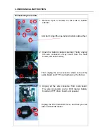

5
5
4
4
3
3
2
2
1
1
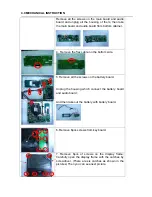
D
D
C
C
B
B
A
A
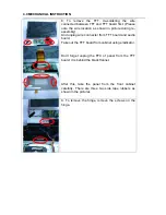
24
T-
TRAY SW
1
Vcc
BC847B
OPU Protection
4
DVD-LD
E
1
2
3
19
HITACHI 1200X
POWER
3
E
1
S
6
10
GND-LD
3
3
HFM
S-FLASH
CD/DVD SW
C
2
IIC
VR-CD
7
MD
17
DRAM
F-
9
GND-PD
F+
B
F
VIDEO INTERFACE
Vc(Vref)
12
16
1
1
PANEL I/F
2
E
T+
2N3904
NC
C
20
G
15
RF
VR-DVD
2SK3018
C/c
22
2
RF Reference
3
21
13
B
CRYSTAL CIRCUIT
2SB1132
B/b
D
23
D/d
2N3906
NC
B
14
8
A/a
C
18
RS-232
E
AUDIO INTERFACE
5
11
Very Important to
reduce Noise
1
C
CD-LD
2
OPO
GPIO2 R56 0R R55NC
OP+ PIN127 R28 0R R29NC
IO
Old
NC
10K
NC
NC
150K
10K
C90
C89
BAT54C
150K
NC
D11
Break circuit
R86
R87
R84
0.1uF
New
0.1uF
0R
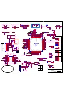
04. MT1389LP LQFP 128
Custom
2
4
Wednesday, May 21, 2008
PET816DVD
Title
Size
Document Number
t
e
e
h
S
:
e
t
a
D
of
FMSO
89
K
P
_V
C
O
M
LD-DVD
T+
S
F_
C
S
TRIN
D
Q
4
R
FV
18
-1
D
Q
6
D
Q
2
MA3
F
RFV18-2
OPO
FMSO
FMSO
FMSO
FMSO
CKV
K2
A
MDI2
SP-
C
V
B
S
D
TRIN
SDA
FOSO
FOSO
FOSO
FOSO
FOSO
FOSO
D
Q
13
AOUT_R
SL-
E
S
TH
L
RFO
FOSO
D
A
C
V
D
D
3
OEH
MA11
D
Q
7
LDO_DVD
V18
AADVDD
U
P
1_
7
G
P
IO
21
F+
UP1_7
S
F_
C
K
LDO_CD
V
R
E
F
MA9
MA7
D
Q
M
0
XI
LIMIT
U
P
1_
6
89KP_VCOM
DQM[0..1]
TRO
IOA
GPIO21
WE#
D
SF_DO
AVDD33
DMO
MA1
SF_CS
C
AOUT_L
MA8
F
VCC
S
F_
D
I
R
FO
89
K
P
_B
K1
A
O
U
T_
R
DQM1
U
R
S
T#
OPO
RFV33
WE#
A
A
D
V
D
D
BL_EN
D
Q
14
OEV
S
F_
D
O
XO
OP-
SCL
D
Q
9
STBY
GPIO8
RFVDD3
SP+
MA2
BA1
89KP_B
GPIO11
F-
STBY
VCC
FMO
SL-
MA6
FMO
K1
DCLK
E
BA0
T-
XI
MO_VCC
TRSO
B
ADACVDD
IR
K3
89
K
P
_R
DACVDD3
TRSO
TRSO
TRSO
TRSO
TRSO
TRSO
RAS#
RAS#
V1P4
CKV
AVCC1
_4
MUTE_DAC
SF_DI
V1P4
D
Q
5
D
Q
11
STVL
SF_CK
T+
MA0
GPIO19
D
Q
1
GPIO11
SDA
A
V
C
M
LD-CD
C
F+
BA0
MA10
STVL
MA4
89KP_R
F-
DMSO
DMSO
DMSO
DMSO
DMSO
DMSO
D
Q
12
RxD
SL+
MA5
APLLVDD3
GPIO7
A
GPIO8
MDI1
FS
FOO
UP1_6
CAS#
D
Q
3
FOO
D
Q
8
O
E
H
MA[0..11]
V20
STHL
URST#
D
Q
15
G
P
IO
19
A
O
U
T_
L
GPIO7
CVBS
DMSO
BA1
CAS#
_3
D
Q
10
D
A
C
V
D
D
3
OEV
TRO
K3
B
DV33
AVDD33
IOA
DCLK
SCL
SL+
RFVDD3
89KP_G
OP+
AVCC1
DMO
V20
CPH1
TxD
89
K
P
_G
DQ[0..15]
AVCC
D
A
C
V
D
D
3
MDI1
D
Q
0
LDO_CD
A
P
LL
V
D
D
3
XO
RFV18-1
RFV18-2
A
D
A
C
V
D
D
IOA
V20
MUTE_DAC
RxD
TxD
K4
GPIO12
Low Voltage Det
Low Voltage Det
LDO_DVD
_2
_1
T-
GPIO12
K4
K2
V1P4
V1P4
V1P4
SP+
OP+
OPO
OPO
OP-
OP-
SP-
V
1P
4
LIMIT
SP-A
CPH1
BL_EN
FG
LIMIT
IR
RFV33
1
CAS#
3
DCLK
3
SF_CK
3
URST#
1
RAS#
3
SDA
3
DQM[0..1]
3
BA0
3
89KP_B
1
WE#
3
STHL
1
DQ[0..15] 3
OEV
1
BA1
3
STVL
1
89KP_R
1
AOUT_R
4
CVBS
4
BL_EN
1
CPH1
1
OEH
1
CKV
1
89KP_G
1
AOUT_L
4
SCL
3
89KP_VCOM
1
MUTE_DAC
4
SF_CS
3
SF_DO
3
DV33
1,3
AVCC
1
MA[0..11]
3
SF_DI
3
VCC
1,4
V18
1
Low Voltage Det1
DV33
MO_VCC
RFVDD3
RFVDD3
89L_3V3
RFV18-1
V18
MO_VCC
AADVDD
AVDD33
APLLVDD3
89L_3V3
RFV18-2
MO_VCC
RFV18-2
V18
AVCC
DV33
RFV33
V18
89L_3V3
RFV33
DACVDD3
89L_3V3
V18
RFV18-1
VCC
AVCC
89L_3V3
DV33
AVDD33
89L_3V3
ADACVDD
DV33
DV33
DV33
DV33
89L_3V3
C60
6800pF
R63
0R
R91
1R
R
35
10
K
+
E
C
25
10
0u
F/
6.
3V
C81
0.1uF
R40
0
L18
FB
L22
NC
R84 10k
R54
0
HA3
4x1
1
2
3
4
R49
2K2 FB
HA2
2x1
1
2
R83
10k
C
67
10
0p
F
C45
0.1uF
R88
0
C86
0.1uF
C50
0.1uF
+
EC21
10uF/16VSMD
R71
1
C89
0.1uF
R
36
10
K
R75
18k
R44
0R
R56
0
R47
10k
U4
BA5954
1
9
10
12
3
2
15
7
14
13
21
19
20
24
27
6
4
5
28
8
11
17
18
16
23
22
25
26
29
30
VINFC
PVCC1
PGND
VOSL+
CF2
CF1
VOTK+
VNFFC
VOFC+
VOFC-
PVCC2
PGND
VNFTK
CTK2
BIAS
VOSL
VINSL+
VINSL-
STBY
VCC
VOSL-
VOLD+
VOLD-
VOTK-
VINLD
PREGND
CTK1
VINTK
G1
G2
R70
1
L23
FB
R
85
68
0K
/N
C
R48
2K2 FB
L32
FB
C15
1U/0603
+
EC23
10uF/6.3VSMD
R78 10k
R76
15k
R42
2K2 FB
J6
5x1
DIP5-1.25
1
2
3
4
5
R
37
10
K
R80
20k
R52
0
C91
2200pF/NC
C
55
0.
1u
F
L29
FB
C
90
0.1
uF
C85
2200pF/NC
C
65
10
0p
F
+
EC22
10uF/16VSMD
R50
10k
R58
0
+
EC29
47uF/16V
R92
0
C73
0.1uF
+
E
C
24
47
0u
F/
10
v
C
5710
uF
/1
6V
S
M
D
C61
0.1uF
C77
0.1uF
R72
1
C
64
10
0p
F
C84 150pF
+
EC27
100uF/10v
C82
0.015uF
C
56
4.
7u
F
R73
1
R51
100k
C41
0.1uF
C38
0.1uF
R66
6.8R
C43
0.1uF
C87 OPEN
Q12
3904
C72
NC
Y1
27MHz
C
58
0.
1u
F
R65
0R
C40
0.1uF
R57
0R
C69
NC
C47
22pF
L20
150uH
C46
22pF
C
59
15
00
pF
L24
FB
C
62
22
0p
F
R79 20k
L25
FB
Q16
2SB1132
2
1
3
C80
330pF
TOP
HA1
HEADER 24 SMD0.5 TOP
1
2
3
4
5
6
7
8
9
10
11
12
13
14
15
16
17
18
19
20
21
22
23
24
C79
330pF
Q15
2SB1132
2
1
3
C44
0.1uF
D11
BAT54C
1
2
3
R89
NC
R1
33R
R81
20k
C54
120pF/NC
C68
0.1uF
Q13
2SK3018
1
3
2
IR1
IR
1 2 3
R77
10k
L28
2K2
C83
150pF
R74
20k
SW1
1
2
4
3
C49
10uF/6.3VSMD
C76
0.1uF
R53
0
R61
0
C70
NC
R82
680K/NC
R59
0
C75
0.1uF
R64
NC
R90
10k
R62
15k
R43
2K2 FB
R45
560R 1%
R38
0R
R39
0R
L30
10uH
R67
6.8R
C71
0.1uF
C88
0.1uF
C78
0.1uF
R60
0
C51
100pF
Q14
2SK3018
1
3
2
R87
0R
R86
10k
R
34
10
K
L19
FB
+
EC30
100uF/6.3V
R55
0
R93
10K
R41
NC
MT1389DLE
LQFP 128
V1.0
Portable
U3
MT1389L/SMD
LQFP128/SMD
5
6
7
8
9
10
11
12
14
15
16
17
18
19
20
21
22
23
24
25
26
27
28
29
30
31
32
33 34
36 37 38 39 40 41 42 43 44 45 46 47 48 49
51 52 53
50
55 56 57
54
58 59
61 62 63
60
64
65
66
67
69
70
99 98 97
96
95
94
90
93
92
91
89
88
84
13
35
86
79
85
83
82
81
80
78
77
76
75
74
68
73
72
71
4
3
2
1
12
8
12
7
12
6
12
5
12
4
12
3
11
7
12
0
11
9
11
8
12
2
11
6
11
5
11
4
11
3
11
2
11
1
11
0
10
9
10
8
10
7
10
6
10
5
10
4
10
3
10
2
10
1
10
0
87
12
1
RFE
RFF
AVDD18
AVDD33
XTALI
XTALO
AGND
V20
REXT
MDI1
MDI2
LDO1
LDO2
AVDD33
DMO
FMO
TRAY_OPEN
TRAY_CLOSE
TRO
FOO
FG / GPIO2
USB_DP
USB_DM
USB_V33
USB_GND
PAD_VRT
USB_V18
G
P
IO
3
/ I
N
T#
G
P
IO
4
S
F_
C
S
_
S
F_
D
O
S
F_
D
I
S
F_
C
K
U
P
1_
6
/ S
C
L
U
P
1_
7
/ S
D
A
IC
E
P
R
S
T#
IR R
D
0
R
D
1
R
D
2
R
D
3
R
D
4
R
D
5
R
D
6
R
D
7
D
V
D
D
33
D
Q
M
0
R
D
15
R
D
14
D
V
D
D
18
R
D
13
R
D
12
R
D
11
R
D
10
R
D
9
D
V
S
S
33
R
D
8
DQM1
RCLK
RA11
RA9
RA8
H
C
K
/
G
P
IO
18
H
S
TL
/G
P
IO
17
H
O
E
/G
P
IO
16
VOE/GPIO15
VCK/GPIO14
VSTU / GPIO13
DVDD18
SPDIF / GPIO12
HSTR / GPIO11
LR / GPIO10
UD / GPIO9
VSTD / GPIO8
DVDD33
V14
G
P
IO
6
RA3
DVSS18
RA2
RA1
RA0
RA10
BA1
BA0
RAS#
CAS#
RWE#
RA4
DVDD33
RA5
RA6
RA7
RFD
RFC
RFB
RFA
R
FH
/
O
P
IN
N
R
FG
/
O
P
IN
P
R
FI
N
/
O
P
O
U
T
R
FI
P
A
G
N
D
18
A
V
D
D
18
A
D
A
C
V
S
S
A
L
/ G
P
IO
1
A
V
C
M
A
R
/
G
P
IO
0
A
D
A
C
V
D
D
2
A
P
LL
C
A
P
A
P
LL
V
D
D
A
A
D
V
D
D
A
K
IN
1
/ G
P
IO
21
/
A
ud
io
_M
ut
e
A
D
V
C
M
/
G
P
IO
20
/
V
C
O
M
A
K
IN
2
/ G
P
IO
19
/
A
ud
io
_M
ut
e
A
A
D
V
S
S R B G
D
A
C
V
D
D
A
D
A
C
V
D
D
B
C
V
B
S
D
A
C
V
S
S
C FS
V
R
E
F
D
A
C
V
D
D
C
GPIO7 / CKE
A
D
A
C
V
D
D
1
CB1
0.1uF
R31
100k
C39
10uF/6.3VSMD
C48
0.1uF
C
66
10
0p
F
+
EC28
47uF/16V
R69
10K
C74
0.1uF
R68
5.1k
C
63
1u
F
L31
10uH
R46
100k
J7
4x1
1
2
3
4
Summary of Contents for PET816/05
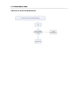
Page 9: ...3 0 INSTRUCTION FOR USE ...
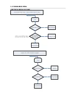
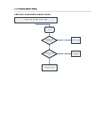
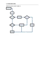
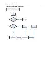
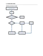
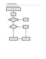
Page 18: ...5 0 TROUBLESHOOTING SYMPTOM NO SOUND FROM HEADPHONE ...
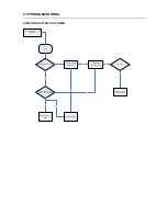
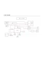
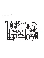
Page 21: ...6 0 BLOCK DIAGRAM ...
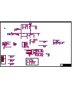
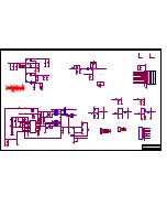
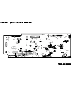
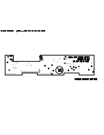
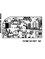
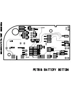
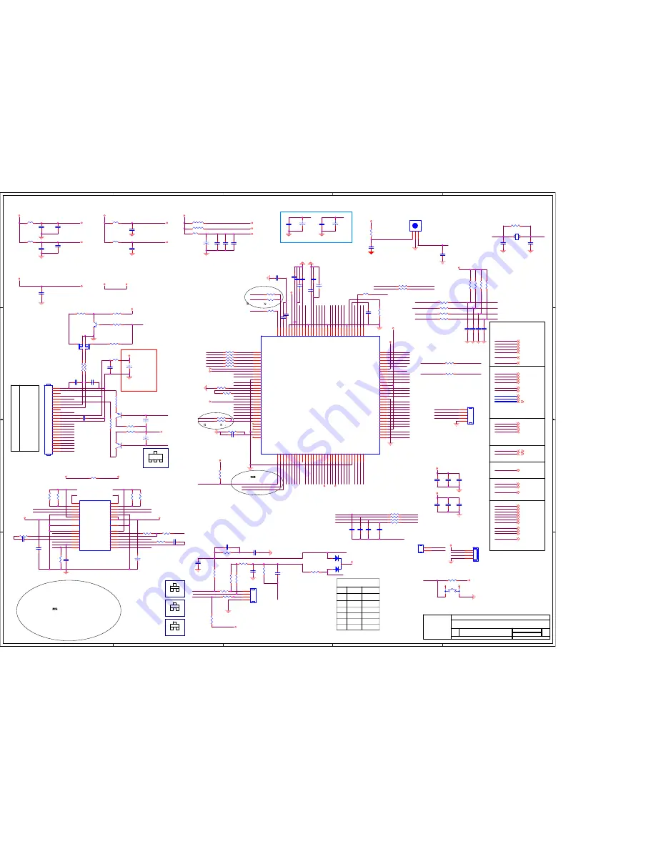
Page 28: ...CIRCUIT DIAGRAM BATTERY 1 1 1 1 ...
Page 29: ......
Page 30: ......
Page 31: ......
Page 32: ......
Page 33: ......
Page 34: ......
Page 35: ......
Page 36: ......