background image

Circuit Descriptions, Abbreviation List, and IC Data Sheets

EN 35

SK4.0A CA

9.

9.

Circuit Descriptions, Abbreviation List, and IC Data Sheets

Index of this chapter:

9.1  Introduction
9.2  The various circuits
9.3  Abbreviation List
9.4  IC Data Sheets

9.1

Introduction

The SK4.0A CA is a CRT TV for the year 2007, based on the 
3P61 platform. In this chapter, only a general description of the 
various circuits is given. For more detailed information, see the 
circuit diagrams in this manual.

9.2

The various circuits

9.2.1

Tuner

The function of the tuner is to select the channel to be received 
and suppress the interference of neighboring channels, to 
amplify the high frequency signal, to improve the receiving 
sensitivity and SNR, and to generate a PIF signal through 
frequency conversion.

9.2.2

IF Channel

The IF Channel mainly ensures the sensitivity and selectivity of 
the complete TV set. The IF AMP integrated in the UOCIII is 
made up of a three-stage dual-differential amplifier with a gain 
value above 70dB, a SNR of 55dB and a bandwidth of 7 MHz. 
The video demodulation circuit is made from the built-in PLL 
Sync Detector. The spectrum of the demodulation carrier is 
unitary and it is not affected by the content of the video signal. 
The tuner features stable receptivity while the signal output 
from the video detector features high fidelity. The built-in PLL 
circuit of the UOCIII generates a 38.0 MHz or 38.9 MHz 
demodulation reference signal for the sync detector to 
demodulate the video signal; this is called "PLL sync 
demodulation".
 

9.2.3

Sound Channel

An external ceramic filter is used to select the second SIF 
signal for the sound channel of UOCIII from the signal output of 
the video detector. The audio signal is obtained after limiting 
amplification and demodulation by the intermediate frequency 
detector for the SIF signal, and then the audio signal is output 
to the audio amplifier TFA9842., which drives the speakers to 
provide the sound. The intermediate frequency detector and 
volume-control attenuator that are built in the UOCIII are set 
and adjusted via the CPU.

9.2.4

CRT Drive Circuit

In the driver circuit, both the voltage and current of the R/G/B 
signal are amplified, after which the CRT drive circuit 
modulates the cathode beam current of the CRT. The R/G/B 
signal input into the driver circuit is of negative polarity.

9.2.5

Power Supply Circuit

The function of the power supply circuit is to supply various 
stabilized operating voltages and to provide protections against 
excessive voltages and currents.

9.3

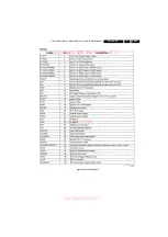
Abbreviation List

2CS

2 Carrier Sound

A2

Commonly known as 2 Carrier Sound 
(2CS) system

AC

Alternating Current

ACI

Automatic Channel Installation: 
algorithm that installs TV channels 
directly from a cable network by 
means of a predefined TXT page

ADC

Analogue to Digital Converter

AFC

Automatic Frequency Control: control 
signal used to tune to the correct 
frequency

AGC

Automatic Gain Control: algorithm that 
controls the video input of the feature 
box

AM

Amplitude Modulation

ANC

Automatic Noise Reduction; One of 
the algorithms of Auto TV

AP

Asia Pacific

AR

Aspect Ratio: 4 by 3 or 16 by 9

AV

Audio Video

AVL

Automatic Volume Level control

B/G

Monochrome TV system. Sound 
carrier distance is 5.5 MHz

BCL

Beam Current Limiter

CBA

Circuit Board Assembly (or PWB)

CFR

Carbon Film Resistor

ComPair

Computer aided rePair

CRT

Cathode Ray Tube (or picture tube)

CVBS

Composite Video Blanking and 
Synchronisation

CVI

Component Video Input

D/K

Monochrome TV system. Sound 
carrier distance is 6.5 MHz. D= VHF-
band, K= UHF-band

DAC

Digital to Analogue Converter

DC

Direct Current

DC-filament

Filament supply voltage

DFU

Directions For Use: owner's manual

DPL

Dolby Pro Logic

DRAM

Dynamic RAM; dynamically refreshed 
RAM

DVD

Digital Versatile Disc

EEPROM

Electrically Erasable and 
Programmable Read Only Memory

EHT

Extreme High Tension; the voltage 
between the cathode and the shadow 
mask that accelerates the electrons 
towards the screen (around 25 kV)

EMI

Electro Magnetic Interference; 
Leakage of high-frequency radiation 
from a transmission medium

EU

EUrope

EW

East West, related to horizontal 
deflection of the set

EW-DRIVE

East -West correction drive signal.

EXT

EXTernal (source), entering the set by 
SCART or by cinches (jacks)

FBL

Fast Blanking: DC signal 
accompanying RGB signals

FE

Front End; Tuner and RF part together

Field

Each interlaced broadcast FRAME is 
composed of two Fields, each Field 
consists of either Odd or Even lines

Filament

Filament of CRT

FM

Field Memory / Frequency Modulation

Frame

A complete TV picture comprising all 
lines (625/525)

FTV

Flat TeleVision

http://jdwxzlw.5d6d.com/?fromuser=森林 


          家电维修资料网 


        免费下载各种维修资料

Summary of Contents for SK4.0A CA

Page 1: ...vice Modes Error Codes and Fault Finding 9 6 Block Diagrams Test Point Overviews and Waveforms Block Diagram Chassis 11 Schematic Overview Chassis 12 7 Circuit Diagrams and PWB Layouts Mono Carrier Power Supply A1 13 21 22 Mono Carrier Line Deflection A2 14 21 22 Mono Carrier Frame Deflection A3 15 21 22 Mono Carrier Tuner IF A4 16 21 22 Mono Carrier AV Switch A5 17 21 22 Mono Carrier Audio Amplif...

Page 2: ...nt conditions Temperature range C 5 to 45 Maximum humidity 90 R H Power consumption Normal operation W 62 Stand by W 3 1 2 Connection Overview Note The following connector colour abbreviations are used acc to DIN IEC 757 Bk Black Bu Blue Gn Green Gy Grey Rd Red Wh White and Ye Yellow 1 2 1 Rear and Side Connections Figure 1 1 Rear and Side Connections Cinch Video CVBS Out Audio Out Ye Video CVBS 1...

Page 3: ...e 1 2 PWB location 9 12 H_17210_028 eps 130607 B A1 A2 A3 A4 A5 A6 CRT PANEL POWER SUPPLY LINE DEFLECTION FRAME DEFLECTION TONE CONTROL Optional A7 AUDIO AMPLIFIER A8 CPU AND DECODER TUNER IF AV I O MONO CARRIER FRONT CONTROL PANEL D SIDE AV PANEL G MAIN SWITCH PANEL E http jdwxzlw 5d6d com fromuser 森林 家电维修资料网 免费下载各种维修资料 ...

Page 4: ...tomer uses the set under normal circumstances for example in a living room the recommended interval is three to five years When a customer uses the set in an environment with higher dust grease or moisture levels for example in a kitchen the recommended interval is one year The maintenance inspection includes the following actions 1 Perform the general repair instruction noted above 2 Clean the po...

Page 5: ...ds strongly to avoid mixed regimes If this cannot be avoided carefully clear the solder joint from old tin and re solder with new tin 2 4 4 Alternative BOM identification In September 2003 Philips CE introduced a change in the way the serial number or production number see Figure 2 2 is composed From this date on the third digit in the serial number example AG2B0335000001 indicates the number of t...

Page 6: ...or Use EN 6 SK4 0A CA 3 3 Directions for Use You can download this information from the following websites http www philips com support http www p4c philips com http jdwxzlw 5d6d com fromuser 森林 家电维修资料网 免费下载各种维修资料 ...

Page 7: ...l Warning disconnect the mains power cord before you remove the rear cover 1 Remove all the fixation screws of the rear cover 2 Now pull the rear cover backwards and remove it Figure 4 1 Rear Cover removal 4 2 Assembly Board Removal 4 2 1 Side I O Panel removal Figure 4 2 Side I O panel removal 1 Disconnect the sidepanel cable from the mono carrier and remove the cable from it s strain reliefs 2 T...

Page 8: ...r the degaussing coil the speakers the front control panel the side I O panel and deflection coil cables Release the main power cord and the side I O panel cable from it s strain reliefs Pull out the mono carrier and place it sidewards This enables the removal of the front control panel 2 Then remove the four fixation screws 1 of the Front Control panel and remove the board 4 3 Set Re assembly To ...

Page 9: ...n t find any TV program Checking method Check the closed circuit from tuner to picture decoder IC to detect whether there are defective components Or check whether the resistance of R117 R118 R203 and R204 has increased which also could cause the problem 5 4 5 No Good Picture or Double Image Check the correctness of the signal from IF1 IF2 to Q101 and relevant circuit In this case the problem can ...

Page 10: ...Service Modes Error Codes and Fault Finding EN 10 SK4 0A CA 5 Personal Notes E_06532_012 eps 131004 http jdwxzlw 5d6d com fromuser 森林 家电维修资料网 免费下载各种维修资料 ...

Page 11: ...43 L R TONE CONTROL KEY CONTROL R G B IK 24C08 CQ0765 V AMP TDA4863AJ H DRIVE SPL SPR CRT BOARD 21 CRT V DY H DY R OUT G OUT B OUT SW 90V 260V DEG COIL POWER SCL SDA PHILIPS UOC2 110V FOR B 43V 12V FOR MAIN 20V FOR AMP CVBS OUT SLIM PART 63 62 4 AV3 SW 10 9 PWM CONTROL AUDIO VOL MUTE AUDIO OUT SCART ID 7 10 44 5 I O 6 KEY L R AV1 SW AV2 SW 1 12 V 2 15 14 5 3 13 AUDIO 3DD5023 4 11 FM 8V FOR UOC SCL...

Page 12: ...EN 12 SK4 0A CA 6 Block Diagrams Test Point Overviews and Waveforms Schematic Overview Chassis H_17210_022 eps 080607 http jdwxzlw 5d6d com fromuser 森林 家电维修资料网 免费下载各种维修资料 ...

Page 13: ...L SR601 VDR601 GAS DISCHARGE L2 PFC 15mH 2 D607 C612 470pF R608 2K2 C603 0 1uF 250V C603 0 22uF D608 D605 D606 2 R602 200K D602 C611 0 1uF R604 39K ZD604 18V R606 6K8 R605 220 C610 10uF C625 1000uF 8 9 10 11 12 13 14 15 16 1 3 4 7 2 6 T603 TRANSFORMER C621 100uF R618 0 22 2W C627 1000uF 25v Q607 C1815 C629 47uF 16V C630 47uF In Out Gnd IC604 L7808 R615 200K V R 6 01 1K C615 0 1U R613 10K TL431 Q60...

Page 14: ... R250 2 2K R316 4 7K D306 8V2 C310 27PF 50V AFC R401 4K7 C314 2n7 2KV L432 790mH C477 4 7uF 8V_VCC AFC AFC FOCUS SCREEN 564 C317 L302 34mH C318 274J 400V C325 364J 400 L301 105mH R321 1K C319 681 1 6 2 9 3 4 8 10 180V 1 2 3 4 T0 CRT GND HEATE R CRT GND 180V R315 4 7K R314 0 22 2W D308 2158 470PF 500V C300 4 7UF 250V C309 5 GND R312 1K C308 0 1U D205 1N4148 C238 4 7U 50V R310 560K D309 1N4148 R318 ...

Page 15: ... D302 BA158 470pF 0 1uF C303 1000uF 25V I NP 7 I NN 6 V out 5 VP4 13V 4 Vp3 pump 3 VP3 2 VP1 13V 1 IC301 TDA4863AJ 5 6 R308 1K8 2W R256 100 C306 0 1uF 100V R307 1 R306 220 2W C305 100uF 50V D304 BA158 C216 CAP C215 CAP 8V R326 10K D301 C302 Q301 C301 R303 C302 C301 R304 220 1W EHT VDRB VDRA v v H_17210_003 eps 110607 FRAME DEFLECTION A3 A3 5800 A3P610 00 http jdwxzlw 5d6d com fromuser 森林 家电维修资料网 免...

Page 16: ... 4 7K C109 10n R113 220 R116 2 2K R110 10 R112 10 C109 0 01U R107 1 2K LC101 NTSC M Q102 C1815 C204 0 01U R114 10K 31 9M 10K R115 Q103 C1815 R213 100 SYSTEM 1 SYSTEM R215 680 C103 10U 16V L101J 1UH SIF SAW102 C703 47 50V IC703 UPC574 R703 10K R102 15K TUNER AGC C105 100U 16V C104 100U 16V L201 10UH R101 27K SYSTEM SYSTEM1 SIF SAW102 33V_BT 8V_VCC TUNER AGC SDA SCL H_17210_004 eps 110607 TUNER IF A...

Page 17: ...L SIDER REAR R REAR L C717 10uF L AUDOUT A2 A1 4052 3 TONE 32 C821 1U 50V 1U 50V C820 C804 10uF C807 10uF OUTR OUTL AUDIOR out AUDIOLout VIDEOOUT BLANK OPTION V R in Y Gin U B in CVBS Y C R831 2 7K TONE26 TONE 7 4052 13 Q803 1815 Q804 1815 Q805 1815 C822 0 1U CVBS Y R835 10K R836 10K AV1 AV2 R837 10K AV3 R829 10 R842 4 7K C823 10U 16V R 8 41 4 7K R 84 0 4 7K R 85 4 1 5K R 85 2 1 5K R 85 5 1 5K Q20...

Page 18: ...0 C901 10U C902 10U R901 10K R902 10K C903 0 47U R903 51K Q901 C1815 R907 1K R904 100K R917 820 R903 51K R920 270 C903 47U C910 0 22U C512 1000U C913 0 01U R905 1K C914 0 1U Q902 R913 510 510 R912 R908 100K R909 100K C909 100U D901 8V2 C CAP C WOODER 8OHM IC901 TFA9800 0 22U C908 C907 0 22U PG SG OUT2 OUT1 MUTE IN IN SVRR VCC 3 2 5 1 4 6 7 9 8 WEIGHT TONE H_17210_006 eps 110607 TONE CONTROL A6 A6 ...

Page 19: ... 7 8 9 1 2 1 2 IC402 TFA9842AJ C424 222D R OUT R770 1K R769 1K VOL L out 22V_VCC RI RO Rout Lout Lin R410 75K 50V R408 3K3 R253 15K C431 10uF 16V D761 1N4148 C432 100uF R407 10K C430 1uF Q402 A1015 C750 1uF C749 1uF C428 47uF 50V C429 220uF 25V C433 1000uF 25V C434 1000UF 25V 4052 13 4050 3 8V_VCC MUTE VOL 22V_VCC H_17210_007 eps 110607 AUDIO AMPLIFIER A7 A7 5800 A3P610 00 http jdwxzlw 5d6d com fr...

Page 20: ...7 33K R425 27K D204 8V2 D202 8V2 D203 8V2 C240 0 022U C241 0 022U R243 22K Q202 C1815 Q203 C1815 GND GND R224 100 R223 180 L206 6 8uH Z201 XT 6 5 Q201 C1815 Z202 XT 6 0 Z204 XT 4 5 GND R227 4K7 R226 4K7 GND Z203 XT 5 5 WP 1 n c 2 A 2 3 V ss 4 V dd 8 PT C 7 SCL 6 SD A 5 IC202 24C08 R204 100 R206 100 C203 0 01U R20 5 3 3K R20 3 3 3K C227 47uF 16V R 20 2 3 3K R231 2 2K R229 390 C246 0 1U 63V R219 47 ...

Page 21: ...Circuit Diagrams and PWB Layouts EN 21 SK4 0A CA 7 Layout Mono Carrier Top Side H_17210_009 eps 080607 5800 A3P610 00 http jdwxzlw 5d6d com fromuser 森林 家电维修资料网 免费下载各种维修资料 ...

Page 22: ...EN 22 SK4 0A CA 7 Circuit Diagrams and PWB Layouts Layout Mono Carrier Bottom Side H_17210_010 eps 080607 5800 A3P610 00 http jdwxzlw 5d6d com fromuser 森林 家电维修资料网 免费下载各种维修资料 ...

Page 23: ...80 1 2 3 4 5 KEYBOARD CIRCUIT L E D SW005 MENU K E Y 5 V I R LED001 LED SW006 SLEEP SW007 MUTE SW008 TV AV SW003 VOL SW002 PRO SW004 VOL SW001 PRO G N D R711 220 R712 330 R713 470 R714 820 R715 1 5K R716 4 7K R717 RES R 100 C 10U R 1K KEYBOARD CIRCUIT D D KEYBOARD CONTROL H_17210_011 eps 080607 5800 D1SL7P 61 http jdwxzlw 5d6d com fromuser 森林 家电维修资料网 免费下载各种维修资料 ...

Page 24: ...grams and PWB Layouts Layout Keyboard Control Panel Top Side Layout Keyboard Control Panel Bottom Side H_17210_012 eps 080607 5800 D1SL7P 61 H_17210_013 eps 080607 5800 D1SL7P 61 http jdwxzlw 5d6d com fromuser 森林 家电维修资料网 免费下载各种维修资料 ...

Page 25: ... PWB Layouts EN 25 SK4 0A CA 7 Main Switch Panel H_17210_014 eps 080607 5800 E1SL7P 61 MAIN SWITCH E E Layout Main Switch Top Side H_17210_015 eps 080607 5800 E1SL7P 61 http jdwxzlw 5d6d com fromuser 森林 家电维修资料网 免费下载各种维修资料 ...

Page 26: ...t Diagrams and PWB Layouts Side A V Panel Layout Side A V Panel 5800 G1SL7P 61 G G SIDE AV H_17210_016 eps 080607 5800 G1SL7P 61 TOP SIDE BOTTOM SIDE H_17210_017 eps 080607 http jdwxzlw 5d6d com fromuser 森林 家电维修资料网 免费下载各种维修资料 ...

Page 27: ... and PWB Layouts EN 27 SK4 0A CA 7 Slim EW Panel H_17210_018 eps 080607 5800 M3P610 00 M M SLIM DEFLECTION Layout Slim EW Panel H_17210_019 eps 080607 5800 M3P610 00 http jdwxzlw 5d6d com fromuser 森林 家电维修资料网 免费下载各种维修资料 ...

Page 28: ...EN 28 SK4 0A CA 7 Circuit Diagrams and PWB Layouts Sub Woofer Panel Optional SUB WOOFER H_17210_020 eps 080607 5800 Z3P610 00 Z Z http jdwxzlw 5d6d com fromuser 森林 家电维修资料网 免费下载各种维修资料 ...

Page 29: ...ircuit Diagrams and PWB Layouts EN 29 SK4 0A CA 7 Layout Sub Woofer Panel H_17210_021 eps 080607 5800 Z3P610 00 Personal Notes E_06532_012 eps 131004 http jdwxzlw 5d6d com fromuser 森林 家电维修资料网 免费下载各种维修资料 ...

Page 30: ...EN 30 SK4 0A CA 7 Circuit Diagrams and PWB Layouts Personal Notes E_06532_013 eps 131004 http jdwxzlw 5d6d com fromuser 森林 家电维修资料网 免费下载各种维修资料 ...

Page 31: ... to other factory menu 8 3 4 Horizontal Adjustment key 1 1 Provide a 50 Hz monoscope pattern Put the set in the MENU mode Press key 1 to enter factory mode 2 Adjust 5HSH for 60 Hz picture its is 6HSH to set picture horizontal centre to CRT horizontal centre 3 Provide a 60 Hz monoscope pattern Put the set in the MENU mode Press key 1 to enter factory mode 4 Adjust 6HSH to set picture horizontal cen...

Page 32: ... P W E 5 4 4 N I M X 0 3 R C U 5 6 8 1 X A M X 9 2 R C L 5 6 4 N I M Y 1 2 T W E 5 1 6 X A M Y 0 4 I M X T 8 3 M Y T 5 CPU EEPROM 070406 CPU EEPROM 070406 CPU EEPROM 070406 2 R L L C 9 2 L S V 5 0 G L L C 6 4 M A V 5 0 R P L C 8 1 L C S 5 0 G P L C 4 3 H S V 5 6 B P L C 8 3 H G R 5 3 R L A W 8 3 F O V 5 0 G L A W 2 4 F O H 0 1 R P A W 2 3 X V 9 G P A W 0 E D I W 0 B P A W 4 V U Y 5 0 D D A H 5 V U...

Page 33: ... 0 Auto sound in auto search mode Bit 1 Off On 0 0 0 1 1 Pan Europe Teletext set Bit 2 Off On 0 0 0 0 0 Cyrillic Teletext set Bit 3 Off On 0 0 0 0 0 Farsi Teletext set Bit 4 Off On 0 0 0 0 0 Arabic Teletext set Bit 5 Off On 0 0 0 0 0 Sync On Y YUV Yprpb mode Bit 6 no yes 1 1 1 1 1 Slicing lever Bit 7 Dependent on noise Fixed 0 0 0 0 0 option 3 191 OP3 0 1 9 9 9 1 1 3P61 Bit 0 Off On 1 1 1 1 1 Engl...

Page 34: ...y XDT Bit 2 XDT 1 bit 4 not applicable XDT 0 bit 4 is valid 1 1 1 1 1 3p or 5p Bit 3 3p 5p 0 0 0 0 0 STB Bit 4 yes no 0 0 0 0 0 When X ray Bit 5 No power off Power off 1 1 1 1 1 Blue black background switch Bit 6 Off On 1 1 1 1 1 Blink power supply indicator Bit7 No flash flash 0 0 0 0 0 option 9 197 OP9 0 1 0 0 0 8 8 FMWS setting When searching Bit0 0 1 0 0 0 0 0 FMWS1 setting When searching Bit1...

Page 35: ...it modulates the cathode beam current of the CRT The R G B signal input into the driver circuit is of negative polarity 9 2 5 Power Supply Circuit The function of the power supply circuit is to supply various stabilized operating voltages and to provide protections against excessive voltages and currents 9 3 Abbreviation List 2CS 2 Carrier Sound A2 Commonly known as 2 Carrier Sound 2CS system AC A...

Page 36: ... West Europe colour carrier 4 433619 MHz and South America colour carrier PAL M 3 575612 MHz and PAL N 3 582056 MHz PCB Printed Circuit Board or PWB PLL Phase Locked Loop Used for e g FST tuning systems The customer can directly provide the desired frequency Progressive Scan Scan mode where all scan lines are displayed in one frame at the same time creating a double vertical resolution PTC Positiv...

Page 37: ...a Sheets This section shows the internal block diagrams and pin layouts of ICs that are drawn as black boxes in the electrical diagrams 9 4 1 Diagram A1 W6554A IC601 Figure 9 1 Block Diagram and Pin Configuration H_17210_039 eps 120607 http jdwxzlw 5d6d com fromuser 森林 家电维修资料网 免费下载各种维修资料 ...

Page 38: ...riptions Abbreviation List and IC Data Sheets EN 38 SK4 0A CA 9 9 4 2 Diagram A1 P412 IC602 Figure 9 2 Block Diagram and Pin Configuration H_17210_039 eps 120607 http jdwxzlw 5d6d com fromuser 森林 家电维修资料网 免费下载各种维修资料 ...

Page 39: ...4865AJ R3 R2 R1 R6 C2 7 INP INN deflection coil from deflection controller VOUT GND VP2 VN VP VP1 VP3 6 5 4 3 2 1 DIFFERENTIAL INPUT STAGE VERTICAL OUTPUT FLYBACK GENERATOR REFERENCE CIRCUIT THERMAL PROTECTION Pin configuration for DBS7P TDA4865AJ TDA4865AJ VP1 VP3 VP2 GND VOUT INN INP 1 2 3 4 5 6 7 Block Diagram Pin Configuration H_17210_038 eps 120607 http jdwxzlw 5d6d com fromuser 森林 家电维修资料网 免费...

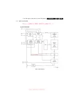
Page 40: ...Circuit Descriptions Abbreviation List and IC Data Sheets EN 40 SK4 0A CA 9 Figure 9 4 Block Diagram H_17210_035 eps 120607 http jdwxzlw 5d6d com fromuser 森林 家电维修资料网 免费下载各种维修资料 ...

Page 41: ...ation List and IC Data Sheets EN 41 SK4 0A CA 9 9 4 4 Diagram A5 4052 IC102 Figure 9 5 Block Diagram and Pin Configuration Block Diagram Pin Configuration H_17210_041 eps 120607 http jdwxzlw 5d6d com fromuser 森林 家电维修资料网 免费下载各种维修资料 ...

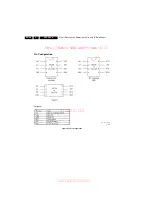
Page 42: ...in Configuration Block Diagram Pin Configuration VOLUME CONTROL SHORT CIRCUIT AND TEMPERATURE PROTECTION VREF 0 5VCC VCC VCC 9 4 IN1 IN2 OUT1 OUT2 SVR CIV VC 1 3 7 8 2 6 5 GND TFA9842AJ 60 kΩ 60 kΩ TFA9842AJ OUT2 CIV IN1 GND SVR VC OUT1 IN2 VCC 2 1 3 4 5 6 7 8 9 H_17210_033 eps 110607 http jdwxzlw 5d6d com fromuser 森林 家电维修资料网 免费下载各种维修资料 ...

Page 43: ...escriptions Abbreviation List and IC Data Sheets EN 43 SK4 0A CA 9 9 4 6 Diagram A8 OM837x IC201 Figure 9 7 Block Diagram H_17210_034 eps 130607 Block Diagram http jdwxzlw 5d6d com fromuser 森林 家电维修资料网 免费下载各种维修资料 ...

Page 44: ...Circuit Descriptions Abbreviation List and IC Data Sheets EN 44 SK4 0A CA 9 Figure 9 8 Pin Configuration H_17210_029 eps 130607 Pin Configuration http jdwxzlw 5d6d com fromuser 森林 家电维修资料网 免费下载各种维修资料 ...

Page 45: ...Circuit Descriptions Abbreviation List and IC Data Sheets EN 45 SK4 0A CA 9 Figure 9 9 Pin Configuration H_17210_030 eps 130607 http jdwxzlw 5d6d com fromuser 森林 家电维修资料网 免费下载各种维修资料 ...

Page 46: ...Circuit Descriptions Abbreviation List and IC Data Sheets EN 46 SK4 0A CA 9 Figure 9 10 Pin Configuration H_17210_031 eps 130607 Pinning http jdwxzlw 5d6d com fromuser 森林 家电维修资料网 免费下载各种维修资料 ...

Page 47: ...rcuit Descriptions Abbreviation List and IC Data Sheets EN 47 SK4 0A CA 9 9 4 7 Diagram A8 24C08 IC202 Figure 9 11 Block Diagram H_17210_035 eps 120607 http jdwxzlw 5d6d com fromuser 森林 家电维修资料网 免费下载各种维修资料 ...

Page 48: ...Circuit Descriptions Abbreviation List and IC Data Sheets EN 48 SK4 0A CA 9 Figure 9 12 Pin Configuration Pin Configuration H_17210_036 eps 120607 http jdwxzlw 5d6d com fromuser 森林 家电维修资料网 免费下载各种维修资料 ...

Page 49: ...V C504 9965 100 04876 0 001µF 10 2kV C508 9965 100 04872 82pF 5 50V C508 9965 100 04875 470pF 10 1kV C509 9965 100 04875 470pF 10 1kV C509 9965 100 05315 47µF 250V C510 9965 100 04875 470pF 10 1kV C516 9965 100 04875 470pF 10 1kV C601 9965 100 04896 0 1uF 250V 500V C602 9965 100 04897 0 22µF 250V 500V C603 9965 000 40565 0 001μF 250V 400V C604 9965 000 40565 0 001μF 250V 400V C605 9965 000 41100 0...

Page 50: ... 100Ω 1 16W R848 9965 000 39977 CFR 100kΩ R849 9965 000 39977 CFR 100kΩ R852 9965 000 40685 CFR 1 5kΩ 1 16W R854 9965 000 40685 CFR 1 5kΩ 1 16W RD2 9965 000 39975 CFR 100Ω 1 16W RD2 9965 100 04851 820Ω 5 1 16 1 6W RD3 9965 000 40693 CFR 2 7kΩ 1 16W RD3 9965 100 04843 3 6kΩ 5 1 16 1 6W RD4 9965 000 39976 CFR 10kΩ 1 16W RD4 9965 000 40686 CFR 15kΩ 1 16W RD5 9965 000 40688 CFR 18kΩ 1 16W RD5 9965 100...

Page 51: ...250V Q601 9965 100 04919 I C AZ431AZ BAAC Q601 9965 100 05321 TL431ALF TL431ALS Ik Q602 9965 100 04913 Transistor 2SC2120Y Q603 9965 000 40232 2SC1815Y 2PC1815 Q604 9965 000 40232 2SC1815Y 2PC1815 Q606 9965 100 04912 Transistor 2SA1013 Q608 9965 000 40231 2SA1015Y 2PA1015 Q801 9965 000 40232 2SC1815Y 2PC1815 Q802 9965 000 40232 2SC1815Y 2PC1815 Q803 9965 000 40232 2SC1815Y 2PC1815 Q804 9965 000 40...

Page 52: ...Revision List EN 52 SK4 0A CA 11 11 Revision List Manual 3122 785 17210 First release http jdwxzlw 5d6d com fromuser 森林 家电维修资料网 免费下载各种维修资料 ...

Reviews: