background image

1999 Oct 12

12

Philips Semiconductors

Product specification

IC card interface

TDA8002C

A

CTIVATION SEQUENCE

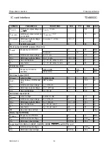
From Idle mode, the circuit enters the activation mode
when the microcontroller sets the CMDVCC line LOW or
sets the MODE line HIGH when the CMDVCC line is
already LOW. The internal circuitry is then activated, the
internal clock is activated and an activation sequence is
executed. When RST is enabled it becomes the inverse of
RSTIN.

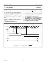
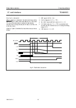
Figures 10 to 12 illustrate the activation sequence as
follows:

1. Step-up converter is started (t

1

t

0

)

2. V

CC

rises from 0 to 3 or 5 V (t

2

= t

1

+ 1

1

2

T) (according

to the state on pin CV/TV)

3. I/O, AUX1 and AUX2 are enabled and CLK is enabled

(t

3

= t

1

+ 4T); I/O, AUX1 and AUX2 were forced LOW

until this time

4. CLK is set by setting RSTIN to HIGH (t

4

)

5. RST is enabled (t

5

= t

1

+ 7T); after t

5

, RSTIN has no

further action on CLK, but is only controlling RST.

The value of V

CC

 (5 or 3 V) must be selected by the level

on pin CV/TV before the activation sequence.

Fig.10  Activation sequence using RSTIN and CMDVCC.

handbook, full pagewidth

FCE273

OSC_INT/64

CMDVCC

VUP

VCC

I/O

CLK

RSTIN

RST

LOW

tact

t0

t1

t2

t3

t4

t5

T = 25 

µ

s

Summary of Contents for TDA8002C

Page 1: ...DATA SHEET Product specification Supersedes data of 1999 Feb 24 File under Integrated Circuits IC02 1999 Oct 12 INTEGRATED CIRCUITS TDA8002C IC card interface ...

Page 2: ...sterCard and Visa compliant Step up converter for VCC generation Supply supervisor for spikes elimination and emergency deactivation Chip select input for easy use of several TDA8002Cs in parallel APPLICATIONS IC card readers for GSM applications Banking Electronic payment Identification Pay TV Road tolling GENERAL DESCRIPTION The TDA8002C is a complete low power analog interface for asynchronous ...

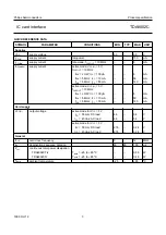
Page 3: ...10 mA 50 mA fCLK 5 MHz ICC 55 mA 140 mA active mode VCC O 3 V fCLKOUT 10 MHz fCLK LOW ICC 100 µA 8 mA fCLK 5 MHz ICC 10 mA 50 mA fCLK 5 MHz ICC 55 mA 140 mA Card supply VCC O output voltage active mode for VCC 5 V ICC 55 mA DC load 4 6 5 4 V ICC 40 nAs AC load 4 6 5 4 V active mode for VCC 3 V ICC 55 mA DC load 2 76 3 24 V ICC 40 nAs AC load 2 76 3 24 V General fCLK card clock frequency 0 12 MHz t...

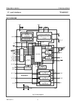
Page 4: ...OR RST BUFFER CLOCK BUFFER SEQUENCER CLOCK CIRCUITRY LATCH OSCILLATOR INTERNAL OSCILLATOR 2 5 MHz STEP UP CONVERTER INTERNAL REFERENCE VOLTAGE SENSE SUPPLY EN2 PVCC EN5 EN4 EN3 CLK EN1 CLKUP ALARM Vref 28 VDDD 13 VDDA 14 12 S1 S2 15 11 VUP AGND 23 VCC 22 RST 18 PRES 21 CLK 20 17 16 AUX1 AUX2 I O 10 29 DGND1 DGND2 32 2 1 I OUC AUX2UC AUX1UC 31 30 9 19 27 24 25 8 5 7 6 XTAL2 XTAL1 CLKOUT 26 STROBE C...

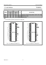
Page 5: ...choosing CLK frequency STROBE 10 10 10 8 I external clock input for synchronous applications CLKOUT 11 11 11 9 O clock output see Table 1 DGND1 12 12 12 10 supply digital ground 1 AGND 13 13 13 11 supply analog ground S2 14 14 14 12 I O capacitance connection for voltage doubler VDDA 15 15 15 13 supply analog supply voltage S1 16 16 16 14 I O capacitance connection for voltage doubler VUP 17 17 17...

Page 6: ...ation TDA8002CT A handbook halfpage XTAL1 XTAL2 I OUC AUX1UC AUX2UC ALARM CLKSEL CLKDIV1 CLKDIV2 STROBE CLKOUT DGND1 AGND S2 MODE RSTIN RST CLK VCC AUX1 AUX2 I O VUP S1 VDDA 1 2 3 4 5 6 7 8 9 10 11 12 13 28 27 26 25 24 23 22 21 20 19 18 17 16 15 14 TDA8002CT A FCE247 OFF CMDVCC PRES Fig 3 Pin configuration TDA8002CT B handbook halfpage XTAL1 XTAL2 I OUC AUX1UC CS ALARM CLKSEL CLKDIV1 CLKDIV2 STROB...

Page 7: ... 6 7 8 9 10 11 12 13 28 27 26 25 24 23 22 21 20 19 18 17 16 15 14 TDA8002CT C FCE249 OFF CMDVCC CV TV PRES Fig 4 Pin configuration TDA8002CT C Fig 5 Pin configuration TDA8002CG handbook full pagewidth TDA8002CG FCE250 1 2 3 4 5 6 7 8 24 23 22 21 20 19 18 17 9 10 11 12 13 14 15 16 32 31 30 29 28 27 26 25 AUX1UC STROBE CLKOUT V DDD I OUC DGND2 AUX2 XTAL2 XTAL1 I O AUX2UC CS ALARM CLKSEL CLKDIV1 CLKD...

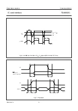
Page 8: ...r up or power down of VDD see Fig 6 This signal is also used for eliminating the spikes on card contacts during power up or power down When VDD reaches Vth2 Vhys2 an internal delay tW is started The ALARM output is active until this delay has expired When VDD falls below Vth2 ALARM is activated and a deactivation sequence of the contacts is performed Clock circuitry The TDA8002C supports both sync...

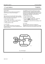
Page 9: ... card interface TDA8002C Fig 6 ALARM as a function of VDD tW pulse width minimum of 10 ms handbook full pagewidth FCE272 VDD tW tW Vth2 Vhys2 Vth2 ALARM Fig 7 Chip select handbook full pagewidth tDZ tSL CS CS INPUTS FCE245 tSI tIS tDI tID OFF I OUC AUX1UC AUX2UC ...

Page 10: ...isables the detection of the falling edge on the other side which becomes slave output see Fig 8 After a delay time td between 50 and 400 ns the logic 0 present on the master side is transferred on the slave side When the input is back to HIGH level a current booster is turned on during the delay td on the output side and then both sides are back to their idle state ready to detect the next logic ...

Page 11: ...ctivation is possible If pin MODE goes LOW in the active mode a normal deactivation sequence is performed before entering the low power mode When pin MODE goes HIGH the circuit enters the normal operating mode after a delay of at least 6 ms 96 cycles of CLKOUT During this time the CLKOUT remains at 16 kHz All card contacts are inactive Oscillator XTAL does not operate The VDD supervisor ALARM outp...

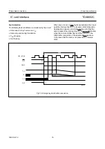
Page 12: ...ate the activation sequence as follows 1 Step up converter is started t1 t0 2 VCC rises from 0 to 3 or 5 V t2 t1 11 2T according to the state on pin CV TV 3 I O AUX1 and AUX2 are enabled and CLK is enabled t3 t1 4T I O AUX1 and AUX2 were forced LOW until this time 4 CLK is set by setting RSTIN to HIGH t4 5 RST is enabled t5 t1 7T after t5 RSTIN has no further action on CLK but is only controlling ...

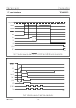
Page 13: ...ence using CMDVCC CLKDIV1 and CLKDIV2 signals to enable CLK handbook full pagewidth FCE274 OSC_INT 64 CMDVCC VUP VCC I O CLK RSTIN RST LOW tact t0 t1 t2 t3 CLKDIV1 CLKDIV2 Fig 12 Activation sequence for synchronous application handbook full pagewidth FCE251 VCC I O AUX1UC AUX1 RSTIN RST STROBE CMDVCC tact CLK ...

Page 14: ...g the sequencer down and thus end in the Idle mode Figures 13 and 14 illustrate the deactivation sequence as follows 1 RST goes LOW t11 t10 2 CLK is stopped t12 t11 1 2T 3 I O AUX1 and AUX2 fall to zero t13 t11 T 4 VCC falls to zero t14 t11 11 2T a special circuit ensures that I O remains below VCC during the falling slope of VCC 5 VUP falls t15 t11 5T handbook full pagewidth FCE479 CMDVCC VUP OSC...

Page 15: ...re detected the circuit pulls the interrupt line OFF to its active LOW state and a deactivation sequence is initiated In the event that the card is present the interrupt line OFF is set to HIGH state when the microcontroller has reset the CMDVCC line HIGH after completion of the deactivation sequence In the event that the card is not present OFF remains LOW handbook full pagewidth FCE480 I O CLK R...

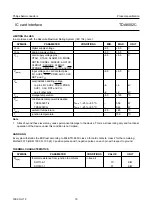
Page 16: ...MBOL PARAMETER CONDITIONS MIN MAX UNIT VDDD digital supply voltage 0 3 6 5 V VDDA analog supply voltage 0 3 6 5 V VCC card supply voltage pins XTAL1 XTAL2 ALARM CS MODE RSTIN CLKSEL AUX2UC AUX1UC CLKDIV1 CLKDIV2 CLKOUT STROBE CMDVCC CV TV and OFF 0 3 6 5 V Vi card input voltage on card contact pins I O AUX2 PRES PRES AUX1 CLK RST and VCC 0 3 6 5 V Ves electrostatic handling voltage on pins I O AUX...

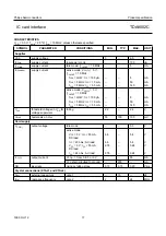
Page 17: ...A active mode VCC O 3 V fCLKOUT 10 MHz fCLK LOW ICC 100 µA 8 mA fCLK 5 MHz ICC 10 mA 50 mA fCLK 5 MHz ICC 55 mA 140 mA Vth2 threshold voltage on VDD for voltage supervisor falling 2 2 2 4 V Vhys2 hysteresis on Vth2 50 100 150 mV Card supply VCC O output voltage Idle mode 0 3 V active mode VCC 5 V ICC 55 mA DC load 4 6 5 4 V ICC 40 nAs AC load 4 6 5 4 V VCC 3 V ICC 55 mA DC load 2 76 3 24 V ICC 24 ...

Page 18: ...data lines outside a session 0 4 V Rpu internal pull up resistance between data lines and VCC 8 10 12 kΩ Iedge current from data lines when active pull up is active 1 mA IIL LOW level input current on data lines VIL 0 4 V 600 µA IIH HIGH level input current on data lines VIH VCC 10 µA DATA LINES I OUC AUX1UC AND AUX2UC WITH 20 KΩ PULL UP RESISTOR CONNECTED TO VDD WHEN CS IS HIGH AND 100 KΩ WHEN CS...

Page 19: ... 32 kHz Card reset output RST VO inact output voltage inactive modes 0 0 3 V td RST delay between RSTIN and RST RST enabled 100 ns VOL LOW level output voltage IOL 200 µA 0 0 3 V VOH HIGH level output voltage IOH 200 µA VCC 0 5 VCC V tr tf rise and fall times CL 30 pF 0 5 ns Card clock output CLK VO inact output voltage inactive modes 0 0 3 V VOL LOW level output voltage IOL 200 µA 0 0 3 V VOH HIG...

Page 20: ...CC 90 mA Timing tact activation sequence duration guaranteed by design see Fig 12 180 220 µs tde deactivation sequence duration guaranteed by design see Fig 14 50 70 100 µs t3 start of the window for sending CLK to the card see Figs 10 and 11 130 µs t5 end of the window for sending CLK to the card see Fig 11 150 µs tIS time from input to select 100 ns tSI time from select to input 1000 ns tID time...

Page 21: ...tal or resonator 2 When the oscillator is stopped in mode 1 XTAL1 is set to HIGH 3 The transition time and duty cycle definitions are shown in Fig 15 4 CLKOUT transition time and duty cycle do not need to be tested 5 PRES and CMDVCC are active LOW RSTIN PRES and CS are active HIGH δ t1 t1 t2 Fig 15 Definition of transition times handbook full pagewidth MGE741 10 90 90 10 tr tf t1 t2 VOH 1 2 VCC VO...

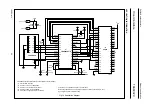
Page 22: ...E PSEN P2 7 P2 6 P2 5 P2 4 P2 3 P2 2 P2 1 P2 0 XTAL1 XTAL2 I OUC AUX1UC CS ALARM CLKSEL CLKDIV1 CLKDIV2 STROBE CLKOUT DGND1 AGND S2 IC2 IC1 MODE OFF RSTIN CMDVCC RST CLK VCC AUX1 PRES I O VUP S1 VDDA VDD 1 2 3 4 5 6 7 8 9 10 11 12 13 28 27 26 25 24 23 22 21 20 19 28 27 26 25 24 23 22 21 30 29 38 37 36 35 34 33 32 31 40 39 18 17 16 15 14 1 2 3 4 5 15 6 7 8 9 10 16 17 18 19 20 11 12 13 14 TDA8002CT ...

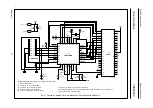
Page 23: ...4 23 22 21 30 29 38 37 36 35 34 33 32 31 40 39 1 2 3 4 5 15 6 7 8 9 10 16 17 18 19 20 11 12 13 14 TDA8002CG C5I C6I C7I C8I C1I C2I C3I C4I C4 C3 C2 C1 C8 C7 C6 C5 1 K1 K2 33 pF 33 pF 14 745 MHz VDD C2 10 µF C1 100 nF VDD J1 1 3 3 V or 5 V J1 2 ground 1 2 3 4 5 6 7 8 AUX1UC STROBE AUX2UC CS ALARM CLKSEL CLKDIV1 CLKDIV2 C4 3 100 nF C5 4 470 nF 24 23 22 21 20 19 18 17 AUX2 RST CLK VCC AUX1 CMDVCC CV...

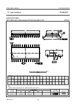
Page 24: ... 25 0 1 DIMENSIONS inch dimensions are derived from the original mm dimensions Note 1 Plastic or metal protrusions of 0 15 mm maximum per side are not included 1 1 0 4 SOT136 1 X 14 28 w M θ A A1 A2 bp D HE Lp Q detail X E Z c L v M A e 15 1 A 3 A y 0 25 075E06 MS 013AE pin 1 index 0 10 0 012 0 004 0 096 0 089 0 019 0 014 0 013 0 009 0 71 0 69 0 30 0 29 0 050 1 4 0 055 0 419 0 394 0 043 0 039 0 03...

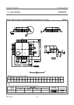
Page 25: ... 9 0 5 7 15 6 85 1 0 0 95 0 55 7 0 o o 0 12 0 1 DIMENSIONS mm are the original dimensions Note 1 Plastic or metal protrusions of 0 25 mm maximum per side are not included 0 75 0 45 SOT401 1 95 12 19 97 08 04 D 1 1 1 5 1 4 9 HD 7 15 6 85 E Z 0 95 0 55 D bp e E B 8 D H bp E H v M B D ZD A ZE e v M A X 1 32 25 24 17 16 9 θ A1 A Lp detail X L A 3 A2 y w M w M 0 2 5 5 mm scale LQFP32 plastic low profil...

Page 26: ...come these problems the double wave soldering method was specifically developed If wave soldering is used the following conditions must be observed for optimal results Use a double wave soldering method comprising a turbulent wave with high upward pressure followed by a smooth laminar wave For packages with leads on two sides and a pitch e larger than or equal to 1 27 mm the footprint longitudinal...

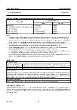
Page 27: ...ch e equal to or smaller than 0 5 mm DEFINITIONS LIFE SUPPORT APPLICATIONS These products are not designed for use in life support appliances devices or systems where malfunction of these products can reasonably be expected to result in personal injury Philips customers using or selling these products for use in such applications do so at their own risk and agree to fully indemnify Philips for any...

Page 28: ... 20052 MONZA MI Tel 39 039 203 6838 Fax 39 039 203 6800 Japan Philips Bldg 13 37 Kohnan 2 chome Minato ku TOKYO 108 8507 Tel 81 3 3740 5130 Fax 81 3 3740 5057 Korea Philips House 260 199 Itaewon dong Yongsan ku SEOUL Tel 82 2 709 1412 Fax 82 2 709 1415 Malaysia No 76 Jalan Universiti 46200 PETALING JAYA SELANGOR Tel 60 3 750 5214 Fax 60 3 757 4880 Mexico 5900 Gateway East Suite 200 EL PASO TEXAS 7...

Reviews: