background image

Philips Semiconductors

TDA9964

12-bit, 3.0 V, 30 Msps analog-to-digital interface for CCD cameras

Objective specification

Rev. 03 — 16 January 2001

12 of 23

9397 750 07918

© Philips Electronics N.V. 2001. All rights reserved.

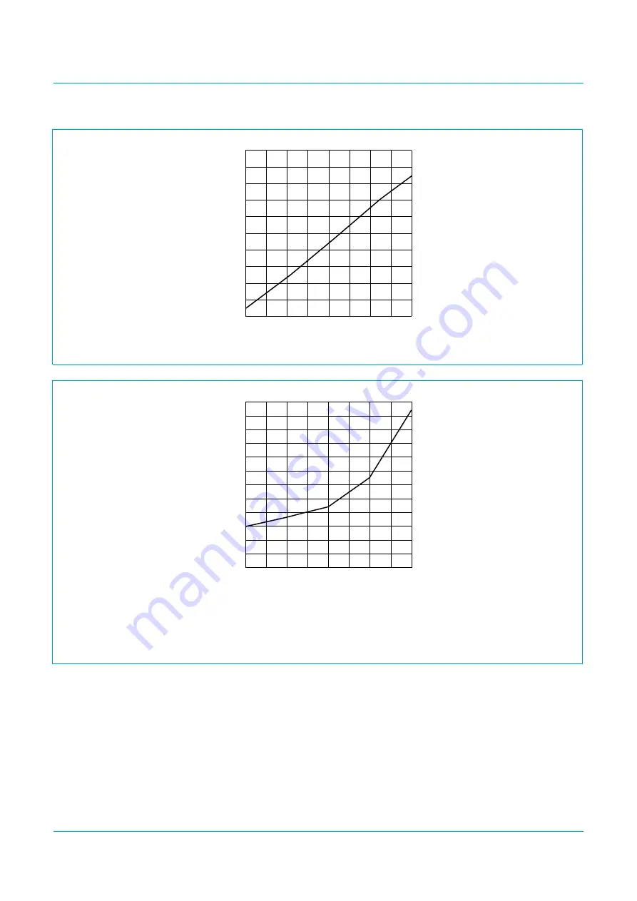
Fig 7.

Total gain from CDS input to ADC input as a function of PGA input code.

0

64

128

255

30

0

1.9

25.9

24

192

PGA input code

TOTAL

gain
(dB)

18

12

6

FCE521

Noise measurement at ADC outputs: Coupling capacitor at input is grounded, so only noise contribution of the front-end is
evaluated. Front-end works at 30 Mpixels with line of 1024 pixels of which the first 40 lines are used to run CLPOB and the
last 40 lines for CLPDM. Data at the ADC outputs is measured during the other pixels. As a result, the standard deviation of the
codes statistic is computed, resulting in the noise. No quantization noise is taken into account as there is no input.

Fig 8.

Typical total noise performance as a function of PGA gain.

handbook, halfpage

0

64

128

255

6

0

4

5

192

PGA code

Ntot(rms)

(LSB)

3

2

1

FCE522

Summary of Contents for TDA9964

Page 1: ...e is 1 0 V p p which is available at pin OFDOUT 2 Features Correlated Double Sampling CDS Programmable Gain Amplifier PGA 12 bit Analog to Digital Converter ADC and reference regulator included Fully programmable via a 3 wire serial interface Sampling frequency up to 30 MHz PGA gain range of 24 dB in steps of 0 1 dB Low power consumption of only 175 mW at 2 7 V Power consumption in standby mode of...

Page 2: ...pply current 3 mA ICCO digital outputs supply current fpix 30 MHz CL 10 pF input ramp response time is 800 µs 1 mA ADCres ADC resolution 12 bits Vi CDS p p maximum CDS input voltage peak to peak value VCC 2 85 V 650 mV VCC 3 0 V 800 mV fpix max maximum pixel frequency 30 MHz fpix min minimum pixel frequency tbf MHz DRPGA PGA dynamic range 24 dB Ntot rms total noise from CDS input to ADC output PGA...

Page 3: ...3 BLK 47 CLK 40 AGND6 2 AGND1 1 VCCA1 41 VCCA4 48 CLPDM 44 CLPOB 45 SHP SHIFT CORRELATED DOUBLE SAMPLING 7 BIT REGISTER 8 BIT REGISTER 8 BIT REGISTER 16 15 OPGA OPGAC 12 6 13 TEST AGND4 AGND5 46 SHD SERIAL INTERFACE 17 18 19 SEN SCLK SDATA 20 VSYNC 42 STDBY PGA CLAMP Vref OFD DAC DATA FLIP FLOP CLAMP TDA9964 OGND1 BLACK LEVEL SHIFT hhhhhhhhhhhhhhhhhhhhhhhhhhhhhhhhhhhhhhhhhhhhhhhhhhhhhhhhhhhhhhhhhh...

Page 4: ...N AGND3 AGND4 VCCA2 CPCDS1 CPCDS2 OFDOUT TEST D5 CLK SHD SHP CLPOB BLK STDBY AGND6 OGND2 OE V CCO2 CLPDM V CCA4 DCLPC OPGAC OPGA AGND5 V CCA3 V CCD1 V CCO1 DGND1 SCLK SEN OGND1 VSYNC SDATA Table 3 Pin description Symbol Pin Description VCCA1 1 analog supply voltage 1 AGND1 2 analog ground 1 AGND2 3 analog ground 2 IN 4 input signal from CCD AGND3 5 analog ground 3 AGND4 6 analog ground 4 VCCA2 7 a...

Page 5: ...t 1 D2 27 ADC digital output 2 D3 28 ADC digital output 3 D4 29 ADC digital output 4 D5 30 ADC digital output 5 D6 31 ADC digital output 6 D7 32 ADC digital output 7 D8 33 ADC digital output 8 D9 34 ADC digital output 9 D10 35 ADC digital output 10 D11 36 ADC digital output 11 MSB OGND2 37 output digital ground 2 VCCO2 38 output supply voltage 2 OE 39 output enable control input LOW outputs active...

Page 6: ...tage difference between VCCA and VCCD 0 5 0 5 V between VCCA and VCCO 0 5 1 2 V between VCCD and VCCO 0 5 1 2 V Vi input voltage referenced to AGND 0 3 7 0 V Io data output current 10 mA Tstg storage temperature 55 150 C Tamb ambient temperature 20 75 C Tj junction temperature 150 C Table 5 Thermal characteristics Symbol Parameter Conditions Value Unit Rth j a thermal resistance from junction to a...

Page 7: ...sconductance 20 mS Correlated Double Sampling CDS Vi CDS p p maximum peak to peak CDS input amplitude video signal VCC 2 85 V 650 mV VCC 3 0 V 800 mV Vreset max maximum CDS input reset pulse amplitude 500 mV Ii IN input current into pin IN at floating gate level tbf tbf µA Ci input capacitance 2 pF tCDS min CDS control pulses minimum active time Vi CDS p p 800 mV black to white transition in 1 pix...

Page 8: ...ating level and CCD dark pixel level 100 100 mV Digital to analog converter OFDOUT DAC VOFDOUT p p additional 8 bit control DAC OFD output voltage peak to peak value Ri 1 MΩ 1 0 V VOFDOUT 0 DC output voltage for code 0 AGND V VOFDOUT 255 DC output voltage for code 255 AGND 1 0 V TCDAC DAC output range temperature coefficient 250 ppm C ZOFDOUT DAC output impedance 2000 Ω IOFDOUT OFD output current ...

Page 9: ...S min tCLKH th IN SHP 0 6 V 0 6 V 0 6 V 0 6 V th IN SHD 2 2 V tCDS min td SHD CLK tsu BLK SHD 2 2 V 2 2 V 2 2 V FCE517 IN SHP SHD CLK DATA BLK th o td o 50 2 2 V N ADC CLAMP CODE N 4 N 1 N 2 N 3 N 4 N 5 N 3 N 2 N 1 hhhhhhhhhhhhhhhhhhhhhhhhhhhhhhhhhhhhhhhhhhhhhhhhhhhhhhhhhhhhhhhhhhhhhhhhhhhhhhhhhhhhhhhhhhhhhh hhhhhhhhhhhhhhhhhhhhhhhhhhhhhhhhhhhhhhhhhhhhhhhhhhhhhhhhhhhhhhhhhhhhhhhhhhhhhhhhhhhhhhhhhh...

Page 10: ... 2 V tCDS min tCLKL th IN SHP 0 6 V 0 6 V 0 6 V 0 6 V th IN SHD 0 6 V 0 6 V tCDS min td SHD CLK tsu BLK SHD 2 2 V 2 2 V 2 2 V FCE518 IN SHP SHD CLK DATA BLK th o td o N 50 ADC CLAMP CODE N 4 N 1 N 2 N 3 N 4 N 5 N 3 N 2 N 1 hhhhhhhhhhhhhhhhhhhhhhhhhhhhhhhhhhhhhhhhhhhhhhhhhhhhhhhhhhhhhhhhhhhhhhhhhhhhhhhhhhhhhhhhh hhhhhhhhhhhhhhhhhhhhhhhhhhhhhhhhhhhhhhhhhhhhhhhhhhhhhhhhhhhhhhhhhhhhhhhhhhhhhhhhhhhhhhh...

Page 11: ...ilips Electronics N V 2001 All rights reserved Fig 5 DAC voltage output as a function of DAC input code FCE519 0 OFDOUT DAC voltage output V 1 0 0 255 OFDOUT control DAC input code Fig 6 Line frequency timing diagram FCE520 BLK active HIGH CLPOB active HIGH CLPDM active HIGH AGCOUT VIDEO OPTICAL BLACK CLPOB WINDOW HORIZONTAL FLYBACK DUMMY VIDEO BLK window CLPDM WINDOW ...

Page 12: ...tputs Coupling capacitor at input is grounded so only noise contribution of the front end is evaluated Front end works at 30 Mpixels with line of 1024 pixels of which the first 40 lines are used to run CLPOB and the last 40 lines for CLPDM Data at the ADC outputs is measured during the other pixels As a result the standard deviation of the codes statistic is computed resulting in the noise No quan...

Page 13: ...NTROL PULSE POLARITY LATCHES LATCH SELECTION SD0 LSB MSB SDATA SCLK SEN SCLK 8 bit DAC FCE523 PGA control ADC clamp control control pulses polarity settings SD2 SD1 SD3 SD4 SD5 12 SD6 SHIFT REGISTER SD7 SD8 SD9 SD10 SD11 8 8 7 10 A0 A1 A2 A3 VSYNC FLIP FLOP FLIP FLOP FLIP FLOP tsu1 tsu2 tsu3 10 ns min thd3 thd4 10 ns min Fig 10 Loading sequence of control input data via the serial interface FCE524...

Page 14: ... 1 initialization SD11 to SD0 0 other addresses test modes Table 8 Polarity settings Symbol Pin Serial control bit Active edge or level SHP and SHD 45 and 46 SD4 1 HIGH 0 LOW CLK 47 SD5 1 rising 0 falling CLPDM 48 SD0 1 HIGH 0 LOW CLPOB 44 SD1 1 HIGH 0 LOW BLK 43 SD3 1 HIGH 0 LOW VSYNC 20 SD8 0 rising 1 falling Table 9 Standby control using pin STDBY Bit SD7 of register 0011 STDBY ADC digital outp...

Page 15: ...ot available 2 Input signals IN SHD and SHP must be adjusted to comply with timing signals th IN SHP and th IN SHD see Section 10 Characteristics Fig 11 Application diagram handbook full pagewidth FCE525 1 2 3 4 5 6 7 8 9 10 11 36 48 47 46 45 44 43 42 41 40 39 38 37 13 14 15 16 17 18 19 20 21 22 23 24 35 34 33 32 31 30 29 28 27 26 12 25 TDA9964 D11 D10 D9 D8 D6 D5 D4 D3 D2 VCCO VCCA1 VCCA2 AGND1 A...

Page 16: ...e and a ground ring protection around these connections can be beneficial Separate analog and digital supplies provide the best solution If it is not possible to do this on the board the analog supply pins must be decoupled effectively from the digital supply pins If the same power supply and ground are used for all the pins the decoupling capacitors must be placed as closely as possible to the IC...

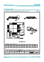
Page 17: ...C JEDEC EIAJ mm 1 60 0 20 0 05 1 45 1 35 0 25 0 27 0 17 0 18 0 12 7 1 6 9 0 5 9 15 8 85 0 95 0 55 7 0 o o 0 12 0 1 0 2 1 0 DIMENSIONS mm are the original dimensions Note 1 Plastic or metal protrusions of 0 25 mm maximum per side are not included 0 75 0 45 SOT313 2 MS 026 136E05 99 12 27 00 01 19 D 1 1 1 7 1 6 9 HD 9 15 8 85 E Z 0 95 0 55 D bp e E B 12 D H bp E H v M B D ZD A ZE e v M A 1 48 37 36 ...

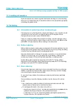
Page 18: ...encilling or pressure syringe dispensing before package placement Several methods exist for reflowing for example convection or convection infrared heating in a conveyor type oven Throughput times preheating soldering and cooling vary between 100 and 200 seconds depending on heating method Typical reflow peak temperatures range from 215 to 250 C The top surface temperature of the packages should p...

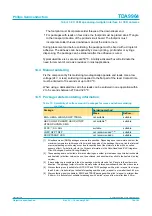
Page 19: ...ing upon the moisture content the maximum temperature with respect to time and body size of the package there is a risk that internal or external package cracks may occur due to vaporization of the moisture in them the so called popcorn effect For details refer to the Drypack information in the Data Handbook IC26 Integrated Circuit Packages Section Packing Methods 2 These packages are not suitable...

Page 20: ... Rev 03 16 January 2001 20 of 23 9397 750 07918 Philips Electronics N V 2001 All rights reserved 15 Revision history Table 14 Revision history Rev Date CPCN Description 03 20010116 Objective specification third version 02 20000801 Objective specification second version 01 20000502 Objective specification initial version ...

Page 21: ...alfunction of these products can reasonably be expected to result in personal injury Philips Semiconductors customers using or selling these products for use in such applications do so at their own risk and agree to fully indemnify Philips Semiconductors for any damages resulting from such application Right to make changes Philips Semiconductors reserves the right to make changes without notice in...

Page 22: ...2 27 09 1412 Fax 82 27 09 1415 Malaysia Tel 60 37 50 5214 Fax 60 37 57 4880 Mexico Tel 9 5 800 234 7381 Middle East see Italy Netherlands Tel 31 40 278 2785 Fax 31 40 278 8399 New Zealand Tel 64 98 49 4160 Fax 64 98 49 7811 Norway Tel 47 22 74 8000 Fax 47 22 74 8341 Philippines Tel 63 28 16 6380 Fax 63 28 17 3474 Poland Tel 48 22 5710 000 Fax 48 22 5710 001 Portugal see Spain Romania see Italy Rus...

Page 23: ... Document order number 9397 750 07918 Contents Philips Semiconductors TDA9964 12 bit 3 0 V 30 Msps analog to digital interface for CCD cameras 1 Description 1 2 Features 1 3 Applications 1 4 Quick reference data 2 5 Ordering information 2 6 Block diagram 3 7 Pinning information 4 7 1 Pinning 4 7 2 Pin description 4 8 Limiting values 6 9 Thermal characteristics 6 10 Characteristics 6 11 Application...

Reviews: