Safety instructions, Modifications
GB 10
VR120
2.
2.
Safety instructions, Modifications
2.1
Safety instructions
•
Safety regulations demand that the set be restored to its
original condition and that components identical with the
original types be used.
•
Safety components are marked by the symbol
h
•
All ICs and many other semi-conductors are susceptible
to electrostatic discharges (ESD). Careless handling
during repair may reduce life drastically. When repairing,
make sure that you are conneted with the same potential
as the mass of the set via a wrist wrap with resistance.
Keep components and tools on the same potential.
•
A set to be repaired should always be connected to the
mains via a suitable isolating transformer.
•
Never replace any modules or any other parts while the
set is switched on.
•
Use plastic instead of metal alignment tools. This in order
to prelude short-circuit or to prevent a specific circuit from
being rendered unstable.
2.1.1
Remarks
•
The direct voltages and oscillograms ought to be
measured relative to the set mass.
•
The direct voltages and oscillograms mentioned in the
diagrams ought to be measured with a colour bar signal
and the picture carrier at 503.25 MHz (C25).
•
The oscillograms and direct voltages have been
measured in RECORD or PLAY mode.
•
The semiconductors, which are mentioned in the circuit
diagram and in the parts lists, are fully exchangeable per
position with the semiconductors in the set, irrespective
of the type designation of these semiconductors.
Engineer's remarks:
Summary of Contents for VR570
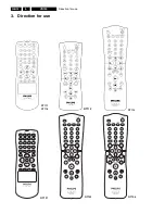
Page 12: ...Direction for use GB 12 VR120 3 3 Direction for use RT111 RT116 RT112 RT114 RT123 RT121 RT128 ...
Page 15: ...Direction for use GB 15 VR120 3 SAT VR870L VR870CC VR720 Set width 435 mm ...
Page 56: ...Service modes Repair tips GB 56 VR120 5 Engineer s remarks ...
Page 79: ...Circuit diagrams and PWB layouts Wiring diagram 79 VR120 7 7 16 Wiring Diagram Motherboard ...
Page 81: ...Circuit diagrams and PWB layouts Wiring diagram 81 VR120 7 Engineer s remarks ...
Page 82: ...82 VR120 7 Circuit diagrams and PWB layouts Wiring diagram Engineer s remarks ...
Page 83: ...Circuit diagrams and PWB layouts Wiring diagram 83 VR120 7 7 18 Mother board component side ...
Page 119: ...Tape deck GB 119 VR120 10 ...
Page 123: ...Tape deck GB 123 VR120 10 Engineer s remarks ...


