Service modes, Repair tips
GB 53
VR120
5.
5.3
Repair tips
5.3.1
Replacement procedure for leadless components (chip)
The following procedures are recommended for replacing
leadless components used in this unit.
1. Preparation for replacement
a.
Soldering iron
Use a pencil-type soldering iron that uses less than 30W
b.
Solder
Use Eutectic solder (Tin 63%, Lead 37%)
c.
Soldering time
Maximum 4 seconds.
Note:
•
Leadless components must not be re-used after removal.
•
Excessive mechanical stress and rubbing of the
component electrode must be avoided.
2. Removing the leadless components
Grasp the leadless component body with tweezers and
alternately apply heat to both electrodes. When the solder on
both electrodes has melted, remove leadless component
with a twisting motion.
Note:
•
Do not attempt to lift the component off the board until the
component is completely disconnected from the board
with a twisting motion.
•
Be careful not to break the copper foil on the printed
circuit board.
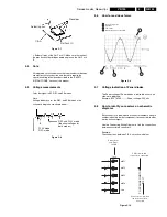
Figure 5-1
3. Installation of leadless components
a. Presolder the contact points on the circuit board
b. Using tweezers press down the part and solder both
electrodes as shown below.
Note:
Do not glue the replacement component to the circuit board.
5.3.2
How to remove/install the Flat Pack IC
How to remove the Flat Pack IC
•
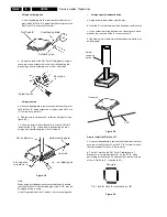
Using a hot air Flat Pack IC unsoldering equipment
Figure 5-2
a. Prepare the hot air Flat Pack IC unsoldering equipment.
Then apply hot air to Flat Pack lC for 5 - 8 seconds.
b. Remove the Flat Pack lC with tweezers while applying the
hot air.
CAUTION:
To avoid damage, do not apply the hot air to the chip parts
around the Flat Pack lC for long periods.
Figure 5-3
Put masking tape around the Flat Pack lC to protect adjacent
parts.
The Flat Pack IC is fixed to the P.C.B. with glue; therefore
take care not to break or damage any foil under the lC or on
each pin when removing it.
Tweezers
Chip
Soldering iron
Soldering iron
Presolder
Tweezers
Soldering iron
Solder
EXAMPLE
C.B.A.
Hot air Flat Pack
IC unsoldering
equipment
Masking
tape
Tweezers
Flat Pack IC
Summary of Contents for VR570
Page 12: ...Direction for use GB 12 VR120 3 3 Direction for use RT111 RT116 RT112 RT114 RT123 RT121 RT128 ...
Page 15: ...Direction for use GB 15 VR120 3 SAT VR870L VR870CC VR720 Set width 435 mm ...
Page 56: ...Service modes Repair tips GB 56 VR120 5 Engineer s remarks ...
Page 79: ...Circuit diagrams and PWB layouts Wiring diagram 79 VR120 7 7 16 Wiring Diagram Motherboard ...
Page 81: ...Circuit diagrams and PWB layouts Wiring diagram 81 VR120 7 Engineer s remarks ...
Page 82: ...82 VR120 7 Circuit diagrams and PWB layouts Wiring diagram Engineer s remarks ...
Page 83: ...Circuit diagrams and PWB layouts Wiring diagram 83 VR120 7 7 18 Mother board component side ...
Page 119: ...Tape deck GB 119 VR120 10 ...
Page 123: ...Tape deck GB 123 VR120 10 Engineer s remarks ...


