Service modes, Repair tips
GB 54
VR120
5.
•
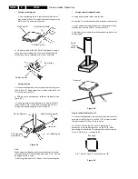
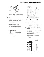
Using a soldering iron
a. Use unsoldering braid to remove the solder from all
pins of the Flat Pack IC. Apply solder flux to all pins of the
Flat Pack IC, to allow easy removal.
b. Lift up each lead of the Flat Pack IC individually, using a
sharp pin or non-solder wire (iron wire), while heating the
pins using a fine tip soldering iron or a hot air blower.
•
Using iron wire
a. Use unsoldering braid to remove the solder from all pins of
the Flat Pack IC. Apply solder flux to all pins of the Flat Pack
IC, to allow easy removal.
b. Affix the wire to workbench or solid mounting point ( see
figure 5-3 )
c. Pull up the wire as the solder melts in order to lift the IC
lead from the P.C.B. contact pad, while heating the pins
using a fine-tip soldering iron or hot air blower.
Figure 5-4
Note:
When using a soldering iron care must be taken to ensure
that the Flat Pack lC is not held by glue or the P.C.B. may be
damaged if force is used.
If the IC is glued, heat the IC with hot air to loosen the glue.
•
Using a special removal device
a. Apply extra tin-lead solder onto the pins
b. Heat the IC to melt the glue which has been used to affix it
c. Use a solder removing device with a special punch which
matches the contours of the IC to remove the IC.
At the other corners there are printed conductors which may
be damaged!
Figure 5-5
How to install the Flat Pack IC
a. Use unsoldering braid to remove the solder from the foil of
each pin of the Flat Pack lC on the P.C.B. in order to install
the replacement Flat Pack IC more easily.
b. The “dot” mark on the Flat Pack IC indicates pin 1.
Make sure this mark matches the 1 on the P.C.B. when
positioning for installation. Then pre-solder the four corners
of the d. Flat Pack IC. ( see figure 5-5 ).
Figure 5-6
Flat Pack IC
Unsoldering braid
Soldering iron
Sharp iron
Soldering iron
Hot air blower
Solid mounting point
Pull up gently
to remove
... or soldering iro
Iron wire
Solder
removing
device
PCB
Control µP
Example
Pin 1 on Flat Pack IC is market by a " ".
Summary of Contents for VR570
Page 12: ...Direction for use GB 12 VR120 3 3 Direction for use RT111 RT116 RT112 RT114 RT123 RT121 RT128 ...
Page 15: ...Direction for use GB 15 VR120 3 SAT VR870L VR870CC VR720 Set width 435 mm ...
Page 56: ...Service modes Repair tips GB 56 VR120 5 Engineer s remarks ...
Page 79: ...Circuit diagrams and PWB layouts Wiring diagram 79 VR120 7 7 16 Wiring Diagram Motherboard ...
Page 81: ...Circuit diagrams and PWB layouts Wiring diagram 81 VR120 7 Engineer s remarks ...
Page 82: ...82 VR120 7 Circuit diagrams and PWB layouts Wiring diagram Engineer s remarks ...
Page 83: ...Circuit diagrams and PWB layouts Wiring diagram 83 VR120 7 7 18 Mother board component side ...
Page 119: ...Tape deck GB 119 VR120 10 ...
Page 123: ...Tape deck GB 123 VR120 10 Engineer s remarks ...


