Service modes, Repair tips
GB 55
VR120
5.
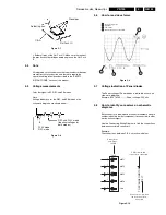
Figure 5-7
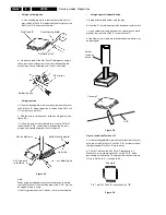
c. Solder all pins of the Flat Pack IC. Make sure that none of
the pins have solder bridges between pins on the Flat Pack
IC.
5.4
Note
All integrated circuits and many other semiconductor devices
are electrostatically sensitive and therefore require the
special handling techniques described in the “SAFETY
INSTRUCTIONS” section of this manual.
5.5
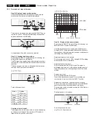
Voltage measurements
Color bar signal in SP REC and PB modes.
Note:
Voltage indications for the REC. and PB mode on the
schematic diagrams are shown below:
Figure 5-8
5.6
How to read wave forms
Figure 5-9
5.7
Voltage indication of Zener diodes
The Zener voltage of Zener diodes is indicated as such on
schematic diagrams:
Example: BZX79C20............Zener voltage: 20 Volts
5.8
How to identify connectors on schematic
diagrams
Each connector is labeled with a connector number and a pin
number indicating to what component it is connected; in other
words, its counterpart.
Use the Connecting Wiring Diagram to find the connections
between associated connectors.
Example:
The connections between C.B.A.s are shown below:
Figure 5-10
Presolder
Soldering iron
C.B.A.
Flat Pack IC
PLAY mode
REC mode
REC and PLAY mode
(identical voltages for
both modes)
Connecting point
Aplitude
Time base
Operating mode of the VCR
1
2
3
4
1
2
3
4
T
O
SCANNER MO
T
O
R
1927
1913
MOT1
MOT3
MOT2
MOT0
POS
1
1
1
1
1
Connector no.
and Pin no.
on PCB
PCB to which this
connector is connected
Connector no. to which
the left connector is
connected
Summary of Contents for VR570
Page 12: ...Direction for use GB 12 VR120 3 3 Direction for use RT111 RT116 RT112 RT114 RT123 RT121 RT128 ...
Page 15: ...Direction for use GB 15 VR120 3 SAT VR870L VR870CC VR720 Set width 435 mm ...
Page 56: ...Service modes Repair tips GB 56 VR120 5 Engineer s remarks ...
Page 79: ...Circuit diagrams and PWB layouts Wiring diagram 79 VR120 7 7 16 Wiring Diagram Motherboard ...
Page 81: ...Circuit diagrams and PWB layouts Wiring diagram 81 VR120 7 Engineer s remarks ...
Page 82: ...82 VR120 7 Circuit diagrams and PWB layouts Wiring diagram Engineer s remarks ...
Page 83: ...Circuit diagrams and PWB layouts Wiring diagram 83 VR120 7 7 18 Mother board component side ...
Page 119: ...Tape deck GB 119 VR120 10 ...
Page 123: ...Tape deck GB 123 VR120 10 Engineer s remarks ...


