Electrical alignments
GB 95
VR120
8.
Determining the deviation (in ppm):
f
mess
..... measured frequency
f
nom
........target frequency (8192,00 Hz)
Deviation = 1x10⁶ x (f
mess
- f
nom
) /
fnom
Determining the correction value for Step 53:
Correction value = Deviation / 0.763 + 128 (round off to whole
number)
The calculated correction value must be between 0 and 255
(change quartz otherwise), and must be entered in Step 53
and saved.
This step can either be exited by performing a main power
source reset, after which the service program must be
entered again or by pressing any key on the set, before
step 53 can be entered.
Example:
f
mess
=8191.97Hz f
nom
=8192.00Hz
Deviation = 1x10
6
x (8191.97 - 8192.00) / 8192.00 = -3.662
Correction value = -3.662 / 0.763 + 128 = 123.20 = 123
8.8.2
Inputing the clock correction
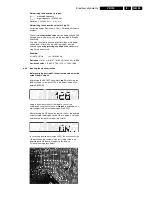
Before carrying out step 53, the correction value must be
established in step 99.
By pressing the SELECT key whilst step 53 is flashing, the
display shows, for instance (128 is the default value of an
empty EEPROM):
Using the numerical keys of the remote control, the
established correction value from Step 99 is entered as a 3-
digit number (value must be between 0 and 255).
After pressing the OK key on the remote control, the entered
code is stored, the display shows OK for approx. 3 seconds
and then the stored value in decimal format.
In case of an invalid entry (value >255), the activation of the
OK key causes the content of the last stored value to be
displayed and OK does not appear in the display.
To leave the step press Select.
Summary of Contents for VR570
Page 12: ...Direction for use GB 12 VR120 3 3 Direction for use RT111 RT116 RT112 RT114 RT123 RT121 RT128 ...
Page 15: ...Direction for use GB 15 VR120 3 SAT VR870L VR870CC VR720 Set width 435 mm ...
Page 56: ...Service modes Repair tips GB 56 VR120 5 Engineer s remarks ...
Page 79: ...Circuit diagrams and PWB layouts Wiring diagram 79 VR120 7 7 16 Wiring Diagram Motherboard ...
Page 81: ...Circuit diagrams and PWB layouts Wiring diagram 81 VR120 7 Engineer s remarks ...
Page 82: ...82 VR120 7 Circuit diagrams and PWB layouts Wiring diagram Engineer s remarks ...
Page 83: ...Circuit diagrams and PWB layouts Wiring diagram 83 VR120 7 7 18 Mother board component side ...
Page 119: ...Tape deck GB 119 VR120 10 ...
Page 123: ...Tape deck GB 123 VR120 10 Engineer s remarks ...


