Circuit descriptions and List of abbreviations
GB 98
VR120
9.
9.1.5
Normal mode:
With the power supply in normal mode, the periodic
sequences in the circuit are divided primarily into the
conductive and blocking phase of the switching transistor
[7302]. During the conductive phase of the switching
transistor [7302], current flows from the rectified mains
voltage to the capacitor [2318] through the primary coil on the
transformer [5301, pins 1-3], the transistor [7302] and
resistors [3314, 3331] to earth ( see figure 9-1 ). The positive
voltage on pin 1 of the transformer [5301] can be assumed to
be constant for a switching cycle. The current in the primary
coil on the transformer [5301] increases linearly in the pattern
of U=L*di/dt. A magnetic field representing a certain volume
of the primary current is formed inside the transformer. In this
phase, the voltages on the secondary coils are polarised in
such a way that the diodes [6300, 6301, 6306, 6308 and
6309] block. From the controller on [7301], a current is
supplied to the CTRL input on the IC [pin 3, 7303] via
optocoupler [7300]. Once the switch-on time for the switching
transistor [7302] has been reached, which corresponds to the
current supplied on the CTRL input, the switching transistor
is switched off.
Once the switching transs been switched off, the blocking
phase begins. No more energy will be transferred into the
transformer. The inductivity of the transformer will still
attempt to maintain the current which has flowed through it
(U=L*di/dt) at a constant level. As the primary current circuit
is interrupted by the shut-off switching transistor [7302], the
current will flow through the secondary coils.
The polarity of the voltages on the transformer is reversed,
which means that the diodes [6300, 6301, 6306, 6308 and
6309] become conductive and current flows into the
capacitors [2301, 2305, 2309, 2311 and 2312] and the load.
This current is also ramp-shaped (di/dt negative, therefore
decreasing).
The control adjustment for the switched-mode power
supply is made by changing the conductive phase of the
switching transistor ( see figure 9-2 ), so that either more or
less energy is transferred from the rectified mains voltage to
[2318] in the transformer. The control information is provided
by the control element [7301]. This element compares the 5V
output voltage via the voltage dividers [3300, 3306, 3336]
with an internal 2.5V reference voltage. The output voltage
from [7301] passes via an optocoupler [7300] (for the metallic
isolation of the primary and secondary parts) as the current
value to pin 3 on the IC [7303]. The switch-on time for the
switching transistor [7302] is inversely proportional to the
value of this current.
9.1.6
Overload, power limitation, burst mode:
With an increasing load on one or more power supply
outputs, the switch-on time for the power transistor [7302]
also increases, and thus also the peak value of the delta-
shaped current through this power transistor. The equivalent
voltage circuit for this current profile is passed from resistors
[3314] and [3331] via [3312] and [3347] to pin 2 on the IC
[7305]. If the voltage on pin 2 reaches 1V in one switching
cycle, the conductive phase of the switching transistor is
ended immediately. This check is made in each individual
switching cycle. This process ensures that no more than
approx. 48W can be taken out of the mains (= power
limitation).
If the power supply reaches the power limit, the output
voltages and the supply voltage Vcc on pin 6 of the IC [7303]
will be reduced following further loading. If Vcc is less than
approx. 10V at any point during this process, the output on
the IC [7303, pin 5] is blocked. All output voltages and Vcc
are reduced. Once Vcc has dropped to below approx. 6.5V,
a new start-up cycle begins. If the overload status or short-
circuit remains, the power limitation will be activated
immediately and the voltages will continue to be reduced,
followed by another start-up attempt ( Burst Mode ). The
amount of power taken up from the mains in burst mode is
low.
9.1.7
Standby mode:
In the ‘Standby‘ operating mode on the device, the ’STBY‘
control line is used to shut off the output voltages 14AL, 5VA
and 5VD on the power supply to minimise the amount of
power taken up from the mains. The supply to the display
heating can also be switched off using the ‘I1WSTBY‘ control
line. The power supply itself will continue to function
continuously in the ‘Standby‘ operating mode with a
switching frequency of 40kHz.
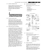
Figure 9-2
9.2
Operating unit DC (DC part)
The microcontroller TMP93CT76F [7899-A] is a 16 bit
microcontroller fitted with 128Kb ROM and 2.5Kb RAM.
It is the core element of the operating unit, fulfilling the
following tasks with the respective functional groups:
•
Integrated VFD driver
•
Timer
•
Evaluation of the keyboard matrix
•
Decoding the remote control commands from the infra-
red receiver pos. 6170
•
Activation of the display
•
Back-up mode
In normal operation, the P is operated in dual-clock mode, i.e.
both quartzes [1170, 1171] oscillate. The time is derived from
the slow quartz [1170] (32.768 kHz), and the fast quartz
[1171] (16MHz) is used to generate the system clock
frequency.
In case of a mains failure (back-up mode) the P is not reset,
but instead the mains failure is registered by the IPOR
interrupt 3 [7899-B] (pin 67) and the P is moved into “Sleep
mode” (low power consumption). The 16MHz quartz is turned
off and the 32kHz quartz is then used as the clock and
system clock frequency. The operating voltage for the AIO is
buffered by a back-up cell [pos. 2174, 2172]. A diode [6171]
prevents this gold capacity from discharging.
UDS
I
D
U
3
= U GS
I
Dmax
point of reversal
t
t
t
Summary of Contents for VR570
Page 12: ...Direction for use GB 12 VR120 3 3 Direction for use RT111 RT116 RT112 RT114 RT123 RT121 RT128 ...
Page 15: ...Direction for use GB 15 VR120 3 SAT VR870L VR870CC VR720 Set width 435 mm ...
Page 56: ...Service modes Repair tips GB 56 VR120 5 Engineer s remarks ...
Page 79: ...Circuit diagrams and PWB layouts Wiring diagram 79 VR120 7 7 16 Wiring Diagram Motherboard ...
Page 81: ...Circuit diagrams and PWB layouts Wiring diagram 81 VR120 7 Engineer s remarks ...
Page 82: ...82 VR120 7 Circuit diagrams and PWB layouts Wiring diagram Engineer s remarks ...
Page 83: ...Circuit diagrams and PWB layouts Wiring diagram 83 VR120 7 7 18 Mother board component side ...
Page 119: ...Tape deck GB 119 VR120 10 ...
Page 123: ...Tape deck GB 123 VR120 10 Engineer s remarks ...


