Circuit descriptions and List of abbreviations
GB 99
VR120
9.
9.2.1
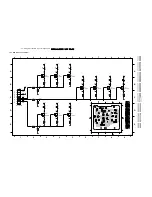
Evaluation of the keyboard matrix
There are 12 different keys. Each key function is assigned a
fixed voltage value. This value is decoded using an
analogue/digital (A/D) port (7899-B, pin 56). Each
mechanical key position on the printed board can adopt any
key function via a coding resistor. Pressing keys
simultaneously may lead to undesired functions!
Schematic:
9.2.2
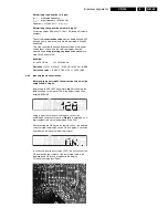
IR receiver and signal evaluation
The IR receiver [6170] includes a selective, controlled
amplifier in addition to a photo-diode. The photo-diode
changes the received transmission (approx. 940nm) in
electrical pulses, which are then amplified and demodulated.
On the output of the IR receiver [7220] a level lift 0V/5V pulse
sequence, which corresponds to the envelope curve of the
received IR remote control command, can be measured. This
pulse sequence is input into the controller for further signal
evaluation via input IRR [7899-B, pin 46].
9.2.3
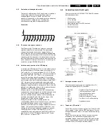
Activation and function of the VFD display
In principle, the VFD display [7170] is a tube triode in which
the heating filaments in the tube serve as cathodes (F+,F-).
The 7 grids (G1 - G7) are activated via PC2 - PC7, PD0 on
the controller, and the 16 anodes (P1 - P16) are controlled via
ports PE0 - PE7, PF0 - PF7, PC0, PC1 on the controller,
each with a positive potential compared to the cathode.
The grids and anodes (digits and symbols to be displayed)
are activated in the time-multiplex procedure, voltage lift 5V/
-18V. A dimmer function is generated using pulse-width
modulation of the grid control signals. At maximum display
brightness, the pulse width for each grid is 2.16 ms. It can be
reduced, controlled using software, which reduces the visual
brightness of the VFD display accordingly.
A digit or symbol is only illuminated if the corresponding
anode and the surrounding grid are switched simultaneously
to 5V for a certain time within a scanning period. The
electrons emitted from the cathode are accelerated by the
positively charged grid and hit the luminous layer of the
anode which is also positively charged.
During the remainder of the scanning period, the
corresponding grid and parts of the anode are at -18V, due to
the internal pull-down resistors in the controller. This
potential is still lower than the average cathode potential of
approx. -15V, prevents the acceleration of electrons, thus
causing the relevant grid and anode segments to go dark.
The heating direct voltage of the display (U = 3.5V) is
supplied from the power supply via lines HELO or HEHI to
pins F+ and F- to the VFD display. Resistors [3070] and
[3071] restrict F- to approx. -15V.
9.3
Central Control AIO (AIO part)
The microcontroller (
µ
C) TMP93CT76F [7899-B] includes
the following functions:
•
PWM outputs
•
A/D converters
•
Composite sync input
•
Special servo inputs for VCR functions
•
I
2
C-BUS interface
•
Shuttle evaluation
9.3.1
Analogue interface to the C:
The following analogue levels are supplied to the
µ
C’s
internal analogue/digital (A/D) converter:
•
TAE/TAS
Tape End / Tape Start Detection
•
TRIV
Tracking Information Video
•
TRIA
Tracking Information Audio
•
AGC
Automatic Gain Control
•
AFC
Automatic Frequency Control
•
8SC1/2
Pin 8 Scart1 or Scart2 switching
voltage
•
Key-in
Keypad evaluation
9.3.2
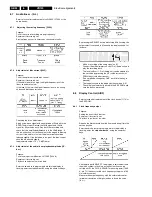
Tape end - LED control :
The LED current is switched using transistor [7804]. The ON
time is approx. 1 msec and the OFF time approx. 12 msec
during playback and 1msec to 5.5msec during the winding
functions.
The LED current is typically 150 mA. In order to prevent
interference from the relatively high pulsed current
‘spreading’ through the entire unit, the LED is fed from the
14VM1, and filtered by 2 resistors [3800, 3805] with 10R
each and a 220
µ
F electrolytic capacitor [2803].
REC
DC-KEY
[7899-B, pin56]
STBY
STOP/EJECT
100K
WIND
REW
MONITOR
STILL
UP
DOWN
STOP
EJECT
PLAY
47K
27K
18K
12K
8K2
5K6
3K9
2K2
1K2
470E
0E
10K
Summary of Contents for VR570
Page 12: ...Direction for use GB 12 VR120 3 3 Direction for use RT111 RT116 RT112 RT114 RT123 RT121 RT128 ...
Page 15: ...Direction for use GB 15 VR120 3 SAT VR870L VR870CC VR720 Set width 435 mm ...
Page 56: ...Service modes Repair tips GB 56 VR120 5 Engineer s remarks ...
Page 79: ...Circuit diagrams and PWB layouts Wiring diagram 79 VR120 7 7 16 Wiring Diagram Motherboard ...
Page 81: ...Circuit diagrams and PWB layouts Wiring diagram 81 VR120 7 Engineer s remarks ...
Page 82: ...82 VR120 7 Circuit diagrams and PWB layouts Wiring diagram Engineer s remarks ...
Page 83: ...Circuit diagrams and PWB layouts Wiring diagram 83 VR120 7 7 18 Mother board component side ...
Page 119: ...Tape deck GB 119 VR120 10 ...
Page 123: ...Tape deck GB 123 VR120 10 Engineer s remarks ...


