background image

L-843e.A1 phyBOARD-Mira i.MX 6 Hardware Manual

© PHYTEC Messtecknik GmbH

23

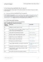
FIGURE 5:  RS-232 or RS

485 Interface Connector X23

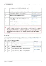
TABLE  9:  Pin Assignment of RS-232 /RS

485 Interface Connector X23

Pin

Signal

Pin

Signal

10

NC

9

GND

8

X_UART3_RS485_B

[3]

7

X_UART3_RS485_A

[3]

6

X_UART3_CTS_RS232

5

X_UART3_TXD_RS232

4

X_UART3_RTS_RS232

3

X_UART3_RXD_RS232

2

NC

1

NC

An adapter cable is included in the phyBOARD

Mira i.MX 6 Kit to facilitate the use of the UART3 interface. The 

following figure shows the signal mapping of the adapter.

Summary of Contents for L-843e.A1

Page 1: ...A product of PHYTEC Technology Holding Company L 843e A1 phyBOARD Mira i MX 6 Hardware Manual ...

Page 2: ...HYTEC Messtecknik GmbH 2 L 843e A1 phyBOARD Mira i MX 6 Hardware Manual Document Title L 843e A1 phyBOARD Mira i MX 6 Hardware Manual Article Number L 843e A1 Release Date 14 07 2000 SBC Prod No PB 01501 xxx CB PCB No 1434 3 1434 4 Edition July 2022 ...

Page 3: ...L 843e A1 phyBOARD Mira i MX 6 Hardware Manual PHYTEC Messtecknik GmbH 3 ...

Page 4: ...Because of that all necessary interfaces are already available on the standard versions thus allowing them to integrate into a large number of applications without modification For any necessary detail adjustment extension connectors are available to enable adding of a wide variety of functions 1 2 Cost optimized with Direct Solder Connect DSC Technology At the heart of the phyBOARD Mira is the ph...

Page 5: ...y Furthermore much of the value of the phyBOARD SBC lies in its layout and test 1 6 Software Support Production ready Board Support Packages BSPs and Design Services for our hardware will further reduce your development time and risk and allow you to focus on your product expertise 1 7 Ordering Information Ordering numbers phyBOARD Mira i MX 6 Development Kit KPB 01501 xxx phyBOARD Mira i MX 6 SBC...

Page 6: ...onnector and serial interface to a host PC 1 11 Product Change Management and Information Regarding Parts Populated on the SOM SBC With the purchase of a PHYTEC SOM SBC you will in addition to our hardware and software possibilities receive free obsolescence maintenance service for the hardware we provide Our PCM Product Change Management team of developers is continuously processing all incoming ...

Page 7: ...pport team through the contact information given within this manual 1 12 PHYTEC Documentation PHYTEC will provide a variety of hardware and software documentation for all of our products This includes any or all of the following QS Guide A short guide on how to set up and boot a phyCORE board along with brief information on building a BSP the device tree and accessing peripherals Hardware Manual A...

Page 8: ...lication Notes and Technical Notes These will be done on a case by case basis Most of the documentation can be found on the applicable download page of our products Tip After finishing the Quickstart Guide we recommend working through the Development Environment Guide This will give you a comprehensive overview of the features and functions of both the SOM and carrier board ...

Page 9: ...e 0 must be added to get the complete address byte E g given address in this manual 0x41 complete address byte 0x83 to read from the device and 0x82 to write to the device Tables that describe jumper settings show the default position in bold blue text Text in blue indicates a hyperlink within or external to the document Click these links to quickly jump to the applicable URL part chapter table or...

Page 10: ...ss jumpers these types of jumpers can be removed and placed by hand with no special tools NC Not Connected NM Not Mounted NS Not Specified PCB Printed circuit board PDI PHYTEC Display Interface defined to connect Phytec display adapter boards or custom adapters PEB PHYTEC Expansion Board PMIC Power management IC PoE Power over Ethernet PoP Package on Package POR Power on reset RTC Real time clock ...

Page 11: ...PHYTEC Messtecknik GmbH 11 Sx User button Sx e g S1 S2 used in reference to the available user buttons or DIP switches on the CB Sx_y Switch y of DIP switch Sx used in reference to the DIP switch on the carrier board VSTBY SOM standby voltage input ...

Page 12: ...D 06 phyBOARD Mira carrier board adding power input buttons connectors signal breakout and Ethernet connectivity amongst other peripherals The PCM 058 System On Module connects to the phyBOARD Mira carrier board by the use of two high density connectors The phyBOARD Mira is also available with the phyCORE i MX 6 in a direct solder form factor PCL 058 a connector less BGA style variant of the PCM 0...

Page 13: ...t out to a Micro SD connector at the backside 1x CAN interface at 2 5 pin header 2 54 mm 1x HDMI interface brought out to a standard type A connector 1x LVDS interface brought out to a 20 pin FFC connector at the backside and separate connector for backlight supply and control 1x One touch interface at 1x4 pin header 2 54 mm 1x LVDS camera interfaces compatible with PHYTEC phyCAM S camera standard...

Page 14: ...L 843e A1 phyBOARD Mira i MX 6 Hardware Manual PHYTEC Messtecknik GmbH 14 3 1 2 Block Diagram FIGURE 1 Block Diagram of the phyBOARD Mira i MX 6 ...

Page 15: ...L 843e A1 phyBOARD Mira i MX 6 Hardware Manual PHYTEC Messtecknik GmbH 15 3 1 3 View of the phyBOARD Mira i MX 6 FIGURE 2 View of the phyBOARD Mira i MX 6 top ...

Page 16: ...L 843e A1 phyBOARD Mira i MX 6 Hardware Manual PHYTEC Messtecknik GmbH 16 FIGURE 3 View of the phyBOARD Mira i MX 6 bottom ...

Page 17: ...ll available connectors on the phyBOARD Mira TABLE 2 phyBOARD Mira Connectors and Pin Headers Reference Designator Description See Section X1 phyCORE Connector 2 x Samtec 2x70 pin X2 Power supply 5 V only via 6 pole WAGO male header or 2 pole Phoenix Contact MINI COMBICON base strip Power Connectors X3 CAN connector 2 5 pin header 2 54 mm pitch CAN Connectivity X4 Ethernet 0 connector RJ45 with sp...

Page 18: ...tage The fourth LED is a user programmable RGB LED View of the phyBOARD Mira i MX 6 top shows the location of the LEDs Their function is listed in the table below TABLE 3 phyBOARD Mira LEDs Descriptions LED Color Description See Section D2 red 3 3 V voltage generation of the phyBOARD Mira Power LED D6 RGB User programmable RGB LED Multicolor RGB LED D13 green Indicates the presence of VBUS at the ...

Page 19: ...he development purposes of the user The function of the removable jumper on the phyBOARD Mira is shown below More detailed information can be found in the appropriate section View of the phyBOARD Mira i MX 6 top shows the location of jumper JP2 TABLE 5 phyBOARD Mira Jumper Description Jumper Description See Section JP2 CAN Termination CAN Connectivity Warning Due to the small footprint of the sold...

Page 20: ...hyBOARDs PEB POW 01 which provides connectivity for 12 V 24 V The required current load capacity for all power supply solutions depends on the specific configuration of the phyCORE mounted on the phyBOARD Mira the particular interfaces enabled while executing software as well as whether an optional expansion board is connected to the carrier board FIGURE 4 Power Supply Connectors X2 Backup Voltage...

Page 21: ...ltage External scaling potential to optimize the electrical output current by use of customized power modules that match the requirements 5 V 3 3 V and backlight power supply Pin assignment of the 6 pole WAGO connector TABLE 7 Pin Assignment of the 6 pole WAGO Connector at X2 Pin Signal Description 1 VCC5V_IN 5 V power supply 2 GND Ground 3 VCC3V3_PMOD 3 3 V power supply 4 VCC_BL Backlight power s...

Page 22: ...ower VCC5V_IN is removed The backup supply for only the RTC U12 lasts approximately 11 days 2 Resistor R117 is not mounted in the standard configuration of the phyBOARD Mira 4 2 2 UART Connectivity X17 and X23 The i MX 6 SOM supports up to 5 so called UART units On the phyBOARD Mira TTL level signals of UART1 and UART2 the standard console are routed to expansion connector X17 UART3 is available a...

Page 23: ...S 485 Interface Connector X23 Pin Signal Pin Signal 10 NC 9 GND 8 X_UART3_RS485_B 3 7 X_UART3_RS485_A 3 6 X_UART3_CTS_RS232 5 X_UART3_TXD_RS232 4 X_UART3_RTS_RS232 3 X_UART3_RXD_RS232 2 NC 1 NC An adapter cable is included in the phyBOARD Mira i MX 6 Kit to facilitate the use of the UART3 interface The following figure shows the signal mapping of the adapter ...

Page 24: ... RS 232 RS 485 Connector Signal Mapping Pin 2 RxD RS232 Pin 3 TxD RS232 Pin 4 A RS485 3 Pin 5 GND Pin 7 RTS RS232 Pin 8 CTS RS232 Pin 9 B RS485 3 3 The standard kit comes with an RS 232transceiver installed If you need an RS 485 interface at X23 instead please contact our sales team ...

Page 25: ...dered with phyCORE i MX 6 module configured for also 1000 Mbps Ethernet and a different RJ45 connector allowing to use the phyBOARD Mira in a 10 100 1000Base T network 4 The LEDs for LINK green and SPEED yellow indications are integrated into the connector The Ethernet transceiver supports Auto MDI X eliminating the need for the consideration of a direct connect LAN or a cross over path cable They...

Page 26: ...ocated next to each other Components Supporting the USB Interfaces FIGURE 7 Components Supporting the USB Interfaces LED D14 displays the status of X_USB1_VBUS and LED D13 the status of X_USB2_VBUS Numerous jumpers configure the USB interfaces according to your needs Please refer to Soldering Jumpers for more information 4 2 4 1 USB Connectivity Rerouting the USB Interfaces to Other Connectors J5 ...

Page 27: ...B_OTG_ID pin to GND forcing the OTG interface into host mode Numerous jumpers allow the USB interfaces to be configured according to your needs Please refer to Soldering Jumpers for more information 4 2 5 CAN Connectivity X3 JP2 The Controller Area Network CAN bus offers a low bandwidth prioritized message fieldbus for serial communication between microcontrollers The Flexible Controller Area Netw...

Page 28: ...n 3 GND Pin 5 Shield Pin 6 GND Pin 7 X_CANH As an alternative option the TTL level signals of FLEXCAN1 can be also routed to expansion port X17 Depending on the muxing options a second CAN interface FLEXCAN2 is available at expansion port X17 4 2 5 1 CAN Connectivity Rerouting the CAN Interface R110 and R111 The first CAN interface FLEXCAN1 can be routed to expansion connector X17 The signals are ...

Page 29: ...ard slot at X22 for connection to SD MMC interface cards It allows easy and convenient connection to peripheral devices like SD and MMC cards Power to the SD interface is supplied by inserting the appropriate card into the MMC SD connector which features card detection a lock mechanism and a smooth extraction function by Push in out of the card DIP switch S2 toggles between NAND boot and boot from...

Page 30: ... a complete overview of the Mini PCI Express connector pin assignment TABLE 16 Mini PCI Express Connector X7 Pin Signal Name Signal Type Signal Level Description 1 X_ECSPI2_MOSI PCIe_nWAKE IN 3 3 V PCIe WAKE 2 VCC3V3 OUT 3 3 V 3 3 V power supply 3 X_ECSPI2_SS0 PCIe_COEX1 I O 3 3 V Coexistence pins for wireless solutions 4 GND Ground 5 X_CSI1_DATA06 PCIe_COEX2 I O 3 3 V Coexistence pins for wireles...

Page 31: ...VD4 Not connected 20 X_EIM_DA14 PCIe_nW_DISABLE OUT 3 3 V Wireless disable signal 21 GND Ground 22 X_ECSPI2_MISO PCIe_nPERST or X_nRESET J12 1 2 OUT 3 3 V Functional card reset by GPIO or X_nRESET 23 X_PCIe_RXN IN DIFF PCIe receive 24 VCC3V3 OUT 3 3 V 3 3 V power supply 25 X_PCIe_RXP IN DIFF PCIe receive 26 GND Ground 27 GND Ground 28 VCC1V5 OUT 1 5 V 1 5 V power supply 29 GND Ground 30 X_I2C1_SCL...

Page 32: ... I O DIFF USB host data 10 11 39 VCC3V3 OUT 3 3 V 3 3 V power supply 40 GND Ground 41 VCC3V3 OUT 3 3 V 3 3 V power supply 42 TP6 IN NS Test point for LED_WWAN 43 GND Ground 44 TP7 IN NS Test point for LED_WLAN 45 RSVD9 Not connected 46 TP8 IN NS Test point for LED_WPAN 47 RSVD10 Not connected 48 VCC1V5 OUT 1 5 V 1 5 V power supply 12 49 RSVD11 Not connected 50 GND Ground 51 RSVD12 Not connected 52...

Page 33: ...protective circuit for the USB interfaces brought out at the Mini PCI Express connector X7 1 2 The 1 5 V voltage can be switched OFF with signal X_CSI1_DATA09 EN_VCC1V5 4 2 8 Camera Connectivity X10 The SOM on the phyBOARD Mira provides two types of camera interfaces parallel and MIPI CSI 2 Generally the parallel port can be expanded on the carrier board in three ways according to the phyCAM P cam...

Page 34: ...K LVDS Clock 7 VCC_CAMERA0 Power supply camera 3 3 V 8 GND Ground 4 2 9 HDMI Connectivity X28 The phyBOARD Mira i MX 6 provides a High Definition Multimedia Interface HDMI which is compliant with HDMI 1 4a DVI 1 0 and HDCP 1 4 It supports a maximum pixel clock of up to 340 MHz for up to 720p at 100 Hz and 720i at 200 Hz or 1080p at 60 Hz and 1080i 720i at 120 Hz HDTV display resolutions and a grap...

Page 35: ... of the protection device FIGURE 13 HDMI Interface Connector X28 4 2 10 LVDS Display Connectivity X9 Meanwhile there are a few LVDS displays on the market with kind of standardized interfaces The LVDS display connector X9 is intended to connect these displays with screen diagonals from 7 up to 12 1 at different resolutions The display connector X9 is a 20 pole receptacle with a 1 mm pitch FIGURE 1...

Page 36: ...LVDS 0 data channel 0 positive output 7 GND Ground 8 X_LVDS0_TX1 OUT 3 3 V LVDS 0 data channel 1 negative output 9 X_LVDS0_TX1 OUT 3 3 V LVDS 0 data channel 1 positive output 10 GND Ground 11 X_LVDS0_TX2 OUT 3 3 V LVDS 0 data channel 2 negative output 12 X_LVDS0_TX2 OUT 3 3 V LVDS 0 data channel 2 positive output 13 GND Ground 14 X_LVDS0_CLK OUT 3 3 V LVDS 0 clock channel negative output 15 X_LVDS...

Page 37: ... the pin assignment and how to set up the right configuration for a custom display refer to LVDS Configurations 4 2 11 Backlight and Display Control Connector X8 In order to support a backlight for the LVDS display X8 provides the supply voltages and control signals necessary FIGURE 15 Backlight and Display Control Connector X8 The following table shows the pinout of the 1 25 mm pitch Molex PanelM...

Page 38: ... interface different provisions are made to connect as well 4 wire resistive touch screens as various capacitive touch screens A touch screen can be connected either to the dedicated touch connector X21 or to the touch signal inputs of the A V connector X13 The following table summarizes the different possibilities available to connect a touch screen to one of these connectors ...

Page 39: ... the phyBOARD Mira i MX 6 top for user applications The colors can be controlled with the following GPIOs TABLE 21 Multicolor LED Configuration Color Signal Description Red X_CSI0_DAT4 GPIO5_IO22 of the i MX 6 Green X_CSI0_DAT5 GPIO5_IO23 of the i MX 6 Blue X_CSI0_DAT6 GPIO5_IO24 of the i MX 6 As an option the LED can be controlled with the LED dimmer IC at U6 14 The LED dimmer can be accessed via...

Page 40: ...le the X_nRESET pin X1D32 of the phyCORE SOM low causing the module to reset FIGURE 18 System Reset Button S1 4 2 16 Audio Video Connectors X13 and X14 The Audio Video A V connectors X13 and X14 provide an easy way to add typical A V functions and features to the phyBOARD Mira Standard interfaces such as parallel display I2 S and I2 C as well as different supply voltages are available at the two A...

Page 41: ...een connectivity as well as an I2 C bus and additional control signals TABLE 23 PHYTEC A V connector X13 Pin Signal Name Signal Type Signal Level Description 1 GND Ground 2 X_LCD_DATA16 OUT 3 3V LCD Data 16 red 0 3 X_LCD_DATA17 OUT 3 3 V LCD Data 17 red 1 4 X_LCD_DATA18 OUT 3 3 V LCD Data 18 red 2 5 X_LCD_DATA19 OUT 3 3 V LCD Data 19 red 3 6 GND Ground 7 X_LCD_DATA20 OUT 3 3 V LCD Data 20 red 4 8 ...

Page 42: ...17 X_LCD_DATA12 OUT 3 3 V LCD Data 12 green 4 18 X_LCD_DATA13 OUT 3 3 V LCD Data 13 green 5 19 X_LCD_DATA14 OUT 3 3 V LCD Data 14 green 6 20 X_LCD_DATA15 OUT 3 3 V LCD Data 15 green 7 21 GND Ground 22 X_LCD_DATA00 OUT 3 3 V LCD Data 00 blue 0 23 X_LCD_DATA01 OUT 3 3 V LCD Data 01 blue 1 24 X_LCD_DATA02 OUT 3 3 V LCD Data 02 blue 2 25 X_LCD_DATA03 OUT 3 3 V LCD Data 03 blue 3 26 GND Ground 27 X_LCD...

Page 43: ...CC_BL OUT NS Backlight power supply 16 40 VCC5V OUT 5 0 V 5 0 V power supply TABLE 24 PHYTEC A V connector X13 Pin Signal Name Signal Type Signal Level Description 1 X_AUD5_TXC I O 3 3 V I S Clock 2 X_AUD5_TXFS I O 3 3 V I S Frame 3 X_AUD5_RXD I O 3 3 V I S Analog Digital converter microphone 4 X_AUD5_TXD I O 3 3 V I S Digital Analog converter speaker 5 X_CSI1_DATA07 AV_INT I O 3 3 V A V interrupt...

Page 44: ...ion Boards in the corresponding application guide L 793e 16 Voltage level is not specified and depends on the connected power module and the attached voltage 17 Note The A V interrupt must be enabled with signal X_CSI1_DATA05_EN_SWITCH GPIO3_04 18 Reset signal depends on J1 please refer to A V Jumper Configuration J1 for more information 4 2 17 Expansion Connector X17 The expansion connector X17 p...

Page 45: ...ply 19 4 GND Ground 5 X_ECSPI1_SS0 OUT 3 3 V SPI 1 chip select 0 6 X_ECSPI1_MOSI OUT 3 3 V SPI 1 master output slave input 7 X_ECSPI1_MISO IN 3 3 V SPI 1 master input slave output 8 X_ECSPI1_SCLK OUT 3 3 V SPI 1 clock output 9 GND Ground 10 X_UART2_RX_DATA IN 3 3 V UART 2 receive data standard debug interface 11 X_I2C1_SDA I O 3 3 V I2C 1 Data 12 X_UART2_TX_DATA OUT 3 3 V UART 2 transmit data stan...

Page 46: ...set 24 GND Ground 25 X_SD3_CMD I O 3 3 V SD MMC command 26 X_SD3_DATA0 I O 3 3 V SD MMC data 0 27 X_SD3_CLK I O 3 3 V SD MMC clock 28 X_SD3_DATA1 I O 3 3 V SD MMC data 1 29 GND Ground 30 X_SD3_DATA2 I O 3 3 V SD MMC data 2 31 X_CSI0_DAT11 ECSPI2_SS0 I O 3 3 V SPI2 chip select 0 UART1 RX GPIO5_29 32 X_SD3_DATA3 I O 3 3 V SD MMC data 3 33 X_CSI0_DAT10 ECSPI2_MISO I O 3 3 V SPI2 MISO UART1 TX GPIO5_2...

Page 47: ...ositive 44 X_CSI0_DAT8 ECSPI2_SCLK OUT 3 3 V SPI 2 clock output J21 1 2 X_SIM_VCC OUT UIM VCC J21 2 3 45 X_SATA_RXN IN DIFF SATA receive negative 46 GND Ground 47 X_FLEXCAN1_TX_EXP OUT 3 3 V CAN 1 transmit data 23 J30 2 3 X_PMIC_nONKEY IN 3 3 V PMIC nONKEY J30 1 2 48 X_FLEXCAN1_RX_EXP IN 3 3 V CAN 1 receive data 23 J31 1 2 49 X_USB_OTG_OC FLEXCAN2_TX OUT 3 3 V CAN 2 transmit data 50 X_USB_OTG_PWR ...

Page 48: ...tion There is no protective circuit for the USB interfaces brought out at the expansion connector X17 22 Caution If the UART2 signals are redirected to these pins the standard console is not available on the Evaluation Board PEB EVAL 01 23 Please refer to CAN Connectivity to make CAN 1 available on the expansion connector 24 The voltage level is not specified and depends on the connected power mod...

Page 49: ...eset signal at A V connector X13 A V Jumper Configuration J1 J5 J6 Rerouting of the USB OTG interface USB1 USB OTG Routing Configuration USB2 USB host Routing Configuration J9 J10 Rerouting of the USB host interface J11 Changing the I2 C address of touchscreen controller U5 J12 Selecting the reset signal at Mini PCIe connector X7 PCIe Connectivity J14 Configuring rising or falling edge strobe for ...

Page 50: ...y Connector Location Mini PCIe connector X7 pin 32 I2C1_SDA pin 30 I2C1_SCL phyCAM S connector X10 pin 4 I2C1_SDA pin 5 I2C1_SCL Expansion connector X17 pin 11 I2C1_SDA pin 13 I2C1_SCL A V connector X13 pin 16 I2C1_SDA pin 15 I2C1_SCL To avoid any conflicts when connecting external I2 C devices to the phyBOARD Mira the addresses of the onboard I2 C devices must be considered The table below lists ...

Page 51: ... 3 LVDS Configurations Various solder jumpers and resistors adapt the pin assignment to different displays If your kit includes a display all jumpers and resistors are preset corresponding to the display The following table gives an overview of possible configurations Please consider the datasheet of the display used to find the right settings TABLE 30 Configuration for LVDS Display Connector X9 P...

Page 52: ...cted 18 X_LVDS_CON FIG4 J18 closed X_LVDS0_TX3 connected open Not connected 19 X_LVDS_CON FIG5 J19 1 2 X_LVDS0_TX3 connected 2 3 High level if R106 26 is mounted Low level if R108 26 is mounted 20 X_LVDS_CON FIG6 J20 1 2 X_LVDS0_TX3 connected 2 3 High level if R105 26 is mounted Low level if R107 26 is mounted 26 All configuration resistors have a value of 10 k ...

Page 53: ...6 Revision History TABLE 31 Date Version Changes in this manual 16 10 2017 Manual L 843e_0 First edition based on the AppGuide L 806e_2 Describes the phyCORE i MX 6 SOM PCB 1429 5 with phyBOARD Mira Carrier Board PCB 1434 3 14 07 2022 Manual L 843e A1 Moved online PDF Version ...

Reviews: