background image

PCM-072/phyCORE-AM64xx System on Module 


  L-860e.A0 


© PHYTEC America L.L.C. 2022 


37 


A current sense amplifier that amplifies the voltage difference, making it easier to measure 


Figure 16. SOM current reader reference circuit 

5.2


Backup Power (VBAT) 

To keep the Real-Time Clock (RTC) module running, a secondary voltage source of 3V can be supplied to the phyCORE-
AM64xx SOM at the VBAT pin (pin B4 of phyCORE-Connector X1). For the RTC to maintain time when main system power 
is removed, the VBAT input must be supplied with power. The RTC draws 40 nA at 3V and is the only draw on VBAT. For 
more information regarding the recommended operating voltage of the Backup Power Source VBAT, refer to 

Table 4

.


5.3 Reset 

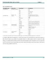
Several reset inputs and outputs are accessible at the phyCORE-Connector as listed in 

Table 13

 below. The X_nRESET_IN, 

X_MCU_RESETz, and X_RESET_REQz can be driven low to trigger cold/warm resets of different domains without cycling 
power on the carrier board. We recommend designing reset buttons into your system that will tie the reset signals to 
ground when pressed, allowing for manual control over system reset. These  buttons  can later be depopulated for 
production purposes but are generally useful during board bring up and verification. 

The X_PWR_EN signal is connected to the enable pin of the PMIC and will prevent the PMIC from starting when pulled 
low. The X_MCU_RESETSTATz, X_RESETSTATz, X_PORz_OUT, and X_PGOOD signals are status outputs. PGOOD indicates 
when the SOM power is stable  and  X_MCU_RESETSTATz  /  X_RESETSTATz  /  X_PORz_OUT are status outputs for 
X_MCU_RESETz / X_RESET_REQz / X_nRESET_IN respectively. 

Table 13 Reset Pin Description 

X1 Pin # 

Signal 

Type 

Level  Description 

B5 

X_PWR_EN 

5V 

Enable pin for PMIC 

B6 

X_nRESET_IN 

3.3V 

Cold system Reset 

B8 

X_MCU_RESETz 

3.3V

1


Warm Reset of MCU Domain 

B11 

X_RESET_REQz 

3.3V

1


Warm Reset of MAIN Domain 

B7 

X_MCU_RESETSTATz 

3.3V

1


MCU Domain Reset Status Output 

B10 

X_PORz_OUT 

3.3V

1


Cold Reset Status Output 

B12 

X_RESETSTATz 

3.3V

1


MAIN Domain Reset Status Output 

Summary of Contents for phyCORE-AM64 Series

Page 1: ...A product of a PHYTEC Technology Holding company phyCORE AM64xx Hardware Manual Document No L 860e A0 SOM Prod No PCM 072 SOM PCB No 1565 1 CB Prod No PBA C 25 CB PCB No 1566 1 Edition Apr 2022...

Page 2: ...sical Dimensions 14 4 3 Connector Alignment for Mating to Carrier Boards 16 4 4 Component Placement Diagram 18 4 5 Technical and Electrical Specifications 20 4 6 Minimum Requirements for Operation 20...

Page 3: ...emory Bus 41 6 2 1 GPMC 41 6 2 2 SD MMC SDIO 43 6 3 System Boot Configuration 45 7 Serial Interfaces 47 7 1 CAN 47 7 1 1 CAN Pinout 47 7 1 2 CAN Reference Circuit 48 7 2 Ethernet 48 7 2 1 Ethernet Pin...

Page 4: ...8 1 Enhanced Capture 73 8 1 1 ECAP Pinout 73 8 2 Enhanced Pulse Width Modulation 74 8 2 1 EPWM Pinout 75 8 3 Enhanced Quadrature Encoder Pulse 76 8 3 1 EQEP Pinout 76 9 Peripheral Interfaces 77 9 1 AD...

Page 5: ...re 6 Top Down View of Mating Connectors 16 Figure 7 Carrier Board Alignment Hole Placement 17 Figure 8 phyCORE AM64xx Component Placement processor side 18 Figure 9 phyCORE AM64xx Component Placement...

Page 6: ...6 Voltage Domain Configurations 22 Table 7 phyCORE AM64xx Connector X1 Column A Pinout 25 Table 8 phyCORE AM64xx Connector X1 Column B Pinout 27 Table 9 phyCORE AM64xx Connector X1 Column C Pinout 28...

Page 7: ...ut Characteristics 72 Table 40 ECAP Connections at the phyCORE Connector 73 Table 41 EPWM Connections at the phyCORE Connector 75 Table 42 EQEP Connections at the phyCORE Connector 76 Table 43 ADC Con...

Page 8: ...C EEPROM 1x SD 3 0 card 1x Independent 1 lane PCIe Gen2 1x USB OTG 2 0 1x USB3 1 Gen1 Dual Role Device 5x 10 100 1000 Mbit Ethernet 1x CPSW provided via on board PHY 4x PRU_ICSSG 2x MCAN with or with...

Page 9: ...conventions used in this manual are as follows Signals that are preceded by an n or end in z e g nRD or RDz are designated as active low signals That is their active state is when they are driven low...

Page 10: ...f jumpers can be removed and placed by hand with no special tools JTAG Joint Test Action Group a serial bus protocol usually used for test purposes LCD Liquid Crystal Display PCB Printed circuit board...

Page 11: ...ut pull up requires an external pull up OD 5V Input PD 5 V tolerant input with pull down 5V_PD LVDS Input Differential line pairs 100 LVDS level input LVDS_I LVDS Output Differential line pairs 100 LV...
Page 12: ...ed focus on hardware peripherals and firmware without expending resources to re invent microprocessor circuitry or other commonly used circuitry that has already been implemented on the phyCORE AM64xx...

Page 13: ...PCM 072 phyCORE AM64xx System on Module L 860e A0 PHYTEC America L L C 2022 13 4 1 Block Diagram Figure 2 phyCORE AM64xx Block Diagram...

Page 14: ...PCM 072 phyCORE AM64xx System on Module L 860e A0 PHYTEC America L L C 2022 14 4 2 Physical Dimensions Figure 3 phyCORE AM64xx Dimensions Top View...

Page 15: ...PCM 072 phyCORE AM64xx System on Module L 860e A0 PHYTEC America L L C 2022 15 Figure 4 phyCORE AM64xx Dimensions Bottom View Figure 5 phyCORE AM64xx Dimensions End View...

Page 16: ...The phyCORE AM64xx has two mounting holes in the lower left and upper right corner sized for M2 5 screws components It is recommended to use the following mounting hardware to secure the SOM to a mati...

Page 17: ...PCM 072 phyCORE AM64xx System on Module L 860e A0 PHYTEC America L L C 2022 17 Figure 7 Carrier Board Alignment Hole Placement...

Page 18: ...Module L 860e A0 PHYTEC America L L C 2022 18 4 4 Component Placement Diagram Figure 8 phyCORE AM64xx Component Placement processor side A searchable pdf of the phyCORE AM64xx component placement proc...

Page 19: ...M64xx System on Module L 860e A0 PHYTEC America L L C 2022 19 Figure 9 phyCORE AM64xx Component Placement connector side A searchable pdf of the phyCORE AM64xx component placement connector side can b...

Page 20: ...null The Yes Command 2 This measurement does not include the current draw from VDD_3V3_OUT of 277mA 3 This measurement does not include the current draw from VDD_3V3_OUT of 290mA 4 6 Minimum Requirem...

Page 21: ...tion of the solder jumpers on the board Table 5 provides a functional summary of the solder jumpers which can be changed to adapt the phyCORE AM64xx SOM to specific design needs It shows their default...

Page 22: ...RG0_PRU1_GPO2 PRG0_PRU1_GPO3 PRG0_PRU1_GPO4 PRG0_PRU1_GPO5 PRG0_PRU1_GPO6 PRG0_PRU1_GPO7 PRG0_PRU1_GPO8 PRG0_PRU1_GPO9 PRG0_PRU1_GPO10 PRG0_PRU1_GPO11 PRG0_PRU1_GPO12 PRG0_PRU1_GPO13 PRG0_PRU1_GPO14 P...

Page 23: ...PCM 072 phyCORE AM64xx System on Module L 860e A0 PHYTEC America L L C 2022 23 Figure 11 Jumper Locations Connector side...

Page 24: ...f the processor pins have multiple multiplexed functions As most of these pins are connected directly to the phyCORE Connector the alternative functions are available by using the phyCORE AM64xx SOM s...

Page 25: ...PWR_I 5 0V Main Power Supply Input A3 VIN PWR_I 5 0V Main Power Supply Input A4 GND Ground A5 GND Ground A6 X_UART0_RTS I O 3 3VJ5 A16 UART Request to Send active low A7 X_UART0_CTS I O 3 3VJ5 B16 UA...

Page 26: ...ansmit Clock A42 X_PRG0_RGMII2_TX_CTL I O 3 3VJ4 U5 PRU RGMII Transmit Control A43 X_PRG0_RGMII2_RX_CTL I O 3 3VJ4 W3 PRU RGMII Receive Control A44 X_PRG0_RGMII2_RXC I O 3 3VJ4 R5 PRU RGMII Receive Cl...

Page 27: ...RT1_CTS I O 3 3VJ5 D16 UART Clear to Send active low B21 X_UART1_RTS I O 3 3VJ5 E16 UART Request to Send active low B22 X_UART1_RX I O 3 3VJ5 E15 UART Receive Data B23 X_UART1_TX I O 3 3VJ5 E14 UART T...

Page 28: ...s listed here but always check the actual jumper setting for the applicable SOM configuration Refer to section 4 6 Solder Jumpers for details J4 The voltage level for this signal is configurable for 1...

Page 29: ...PMC Chip Select 2 active low C27 X_GPMC0_ OEn_REn I O 3 3VJ6 R18 GPMC Output Enable active low or Read Enable active low C28 X_GPMC0_ BE0n_CLE I O 3 3VJ6 P17 GPMC Lower Byte Enable active low or Comma...

Page 30: ...signal is configurable for 1 8V or 3 3V via J6 The default voltage level is listed here but always check the actual jumper setting for the applicable SOM configuration Refer to section 4 6 Solder Jum...

Page 31: ...Data 0 D44 X_MCU_SPI0_CLK I O 3 3VJ2 E6 SPI Clock D45 GND Ground D46 X_MCU_SAFETY_ERRORn I O 1 8V A20 Error signal output from MCU Domain ESM D47 X_MCU_SPI0_CS0 I O 3 3VJ2 D6 SPI Chip Select 0 D48 X_M...

Page 32: ...rnet PHY is populated 4 10 Thermal Management Thermal management is necessary to ensure proper operation of the phyCORE AM64xx SOM especially when integrated inside of an enclosure as the AM64xx proce...

Page 33: ...ute the two traces of a differential pair on the same layer s Route signals over an adjacent solid ground reference plane Ensure there are no layers between the routing layer and reference layer Avoid...

Page 34: ...and routing any other interfaces This is recommended to ensure that the stricter trace lengths and length matching requirements of these interfaces are met Place and route the remaining interfaces af...

Page 35: ...acity is required These pins are A1 A2 and A3 on the X1 connector In our own testing the current draw of the SOM did not exceed 2A but it is important to perform a power analysis to determine how much...

Page 36: ...d to the primary power circuit Figure 15 is a protection circuit that prevents overloads in current voltage from damaging the regulator It contains A power socket for connecting an external power sour...

Page 37: ...ins without cycling power on the carrier board We recommend designing reset buttons into your system that will tie the reset signals to ground when pressed allowing for manual control over system rese...

Page 38: ...Therefore the peripheral carrier board power should be switched on enabled by the X_PGOOD signal to avoid powering external peripherals and circuits that directly interface with the phyCORE AM64xx SO...

Page 39: ...ower If sudden power loss is a concern in your system then consider designing a battery backup or other similar failsafe solution An appropriate battery backup provides enough temporary power for the...

Page 40: ...r Refer to the AM64xx Technical Reference Manual about accessing and configuring these registers Contact our sales team for information on the available DDR4 population options https PHYTEC com contac...

Page 41: ...O 3 3V1 GPMC Data Bus Signal Direction Control GPMC0_OEn_REn C27 X_GPMC0_OEn_REn O 3 3V1 GPMC Output Enable active low or Read Enable active low GPMC0_WEn C17 X_GPMC0_WEn O 3 3V1 GPMC Write Enable ac...

Page 42: ...GPMC Address 22 Output GPMC0_AD0 D3 X_GPMC0_AD0 BOOTMODE_03 100K pullup pulldown network I O 3 3V1 GPMC Data 0 Input Output GPMC0_AD1 D2 X_GPMC0_AD1 BOOTMODE_13 100K pullup pulldown network I O 3 3V1...

Page 43: ...D3 I O 3 3V1 GPMC Data 30 Input Output GPMC0_AD31 C67 X_PRG1_RGMII1_TX_CTL I O 3 3V1 GPMC Data 31 Input Output GPMC0_BE0n_CLE C28 X_GPMC0_BE0n_CLE O 3 3V1 GPMC Lower Byte Enable active low or Command...

Page 44: ...onfiguration Refer to section 4 6 Solder Jumpers for details 6 2 2 2 MMC1 Design In Considerations MMC1 signals should be length matched within 12700 m as described in Table 16 Keep MMC1 trace lengths...

Page 45: ...power on reset cycle the operational system boot mode of the phyCORE AM64xx SOM is determined by the configuration of the BOOTMODE 15 0 signals The BOOTMODE signals must be held at the desired configu...

Page 46: ...is internal Boot flash is oon XXX_1001 Default eMMC boot 1X0_1000 SDIO boot in filesystem mode 1X1_1000 SDIO boot in raw mode BOOTMODE 2 0 PLL Reference Clock selection 000 19 2 MHz 001 20 MHz 010 24...

Page 47: ...tions conforming with CAN protocol version 2 0 part A B and ISO 11898 1 2015 7 1 1 CAN Pinout Table 18 MCAN Connections at the phyCORE Connector X1 Pin s SOM Signal s Type Level Description B17 X_MCAN...

Page 48: ...ible at the phyCORE Connector This Ethernet PHY o Supports 10 BASE Te 100BASE TX and 1000BASE T protocols to interface directly to twisted pair media through an external transformer o Provides two LED...

Page 49: ...Y OD 3 3V LED Link Signal B41 X_CPSW_ETH0_LED_LINK OD 3 3V LED Activity Signal B42 X_CPSW_ETH0_GPIO_0 I O 3 3V SOM Ethernet PHY GPIO 0 B37 X_CPSW_ETH0_A ETH_I O Differential Ethernet Data A Negative B...

Page 50: ...XC A61 X_ PRG0_RGMII1_TXC I O 3 3V1 PRG0 RGMII1 Transmit Clock PRG0_RGMII1_TD0 A56 X_ PRG0_RGMII1_TD0 O 3 3V1 PRG0 RGMII1 Transmit Data 0 PRG0_RGMII1_TD1 A57 X_ PRG0_RGMII1_TD1 O 3 3V1 PRG0 RGMII1 Tra...

Page 51: ...3V1 PRG1 RGMII2 Receive Data 3 RGMII2_RD3 C37 X_CPSW_RGMII2_RD3 I 3 3V1 CPSW RGMII2 Receive Data 3 PRG1_RGMII2_TX_CTL C46 X_CPSW_RGMII2_TX_CTL O 3 3V1 PRG1 RGMII2 Transmit Control RGMII2_TX_CTL C46 X_...

Page 52: ..._IEP0_EDC_LATCH_IN1 B67 X_PRG0_PRU0_GPO7 I 3 3V1 PRU Industrial Ethernet Distributed Clock Latch Input PRG0_IEP0_EDC_SYNC_OUT0 B61 X_PRG0_PRU0_GPO19 O 3 3V1 PRU Industrial Ethernet Distributed Clock S...

Page 53: ...ethernet PHY is populated 7 2 2 Ethernet Design In Guide 7 2 2 1 CPSW_ETH0 Ethernet Design In Considerations Connecting the phyCORE AM64xx SOM to an existing 10 100 1000Base T network involves adding...

Page 54: ...ach individual data and control signal should not fall below the 1ns minimum or exceed the 2 6ns maximum Ensure signals are properly length matched to meet these RGMII timing specifications The follow...

Page 55: ...RXD2 RXD3 1 8ns PRG0_RGMII1_RXCTL 19963 2540 m PRG0_RGMII1_RXD0 19906 PRG0_RGMII1_RXD1 20135 PRG0_RGMII1_RXD2 19924 PRG0_RGMII1_RXD3 20223 Table 25 phyCORE AM64xx PRG0_RMGII2 Trace Length Characteris...

Page 56: ...1_RXD1 41913 PRG1_RGMII1_RXD2 41907 PRG1_RGMII1_RXD3 42173 Table 27 phyCORE AM64xx PRG1_RMGII2 Trace Length Characteristics Signal Name SOM Trace Length m Match Group Recommended Length Match PRG1_RGM...

Page 57: ...l Name SOM Trace Length m Match Group Recommended Length Match RGMII2_TXC 43684 RGMII2 Transmit1 AVERAGE_LENGTH TXCTL TXD0 TXD1 TXD2 TXD3 1 8ns RGMII2_TXCTL 36939 2540 m RGMII2_TXD0 34758 RGMII2_TXD1...

Page 58: ...uits for connecting the CPSW_RGMII1 differential signals from the on board PHY to an RJ45 connector and PRG0_RGMII1 signals to an Ethernet PHY are shown below Figure 22 RJ45 Reference Schematic The ci...

Page 59: ...PCM 072 phyCORE AM64xx System on Module L 860e A0 PHYTEC America L L C 2022 59...

Page 60: ...PCM 072 phyCORE AM64xx System on Module L 860e A0 PHYTEC America L L C 2022 60...

Page 61: ...45 jack for connection to external networks A jumper between TX_CLK1 used when the PHY is MII mode and GTX_CLK1 used when the PHY is in RGMII mode A clock fanout buffer to distribute the reference clo...

Page 62: ...22 X_GPMC0_WAIT1 O 3 3V1 FSI Data FSI_RX2_CLK D3 X_GPMC0_AD0 BOOTMODE_02 100K pullup pulldown network I 3 3V1 FSI Clock FSI_RX2_D0 D2 X_GPMC0_AD1 BOOTMODE_12 100K pullup pulldown network I 3 3V1 FSI D...

Page 63: ...V1 MCU I2C0 Data MCU_I2C0_SCL D29 X_MCU_I2C0_SCL OD O 3 3V1 MCU I2C1 Clock MCU_I2C0_SDA D28 X_MCU_I2C0_SDA OD I O 3 3V1 MCU I2C1 Data I2C0_SCL B52 X_I2C0_SCL 2 2K pullup OD O 3 3V1 Main I2C0 Clock I2C...

Page 64: ...ails 7 5 2 PCIe SERDES Design In Considerations The PCIe subsystem allows for up to 1x single lane PCIe port An external clock is required to drive the PCIe reference clock inputs X_SERDES0_REFCLK0_P...

Page 65: ...PCM 072 phyCORE AM64xx System on Module L 860e A0 PHYTEC America L L C 2022 65 Figure 24 PCIe Reference Schematics...

Page 66: ..._CS1 D21 X_SPI1_CS1 I O 3 3V1 SPI1 Chip Select 1 SPI1_CS2 B20 X_UART1_CTS I O 3 3V1 SPI1 Chip Select 2 SPI1_CS3 B21 X_UART1_RTS I O 3 3V1 SPI1 Chip Select 3 SPI1_D0 D19 X_SPI1_D0 O 3 3V1 SPI1 Data Out...

Page 67: ...s 2 Do not use this signal if the on board ethernet PHY is populated 7 7 UART The Universal Asynchronous Receiver Transmitter module is a slave peripheral that utilizes direct memory access DMA for da...

Page 68: ...K pullup pulldown network UART3_CTSN C8 X_GPMC0_AD9 BOOTMODE_93 100K pullup pulldown network I 3 3V1 UART3 Clear to Send A30 X_MMC1_SDCD 10K pullup A66 X_PRG0_RGMII1_RD3 UART3_RTSN C3 X_GPMC0_AD5 BOOT...

Page 69: ...RD2 O 3 3V1 UART5 Request to Send C17 X_GPMC0_Wen UART5_RXD A37 X_PRG0_RGMII2_TD2 I 3 3V1 UART5 Receive Data D18 X_MCAN1_TX A30 X_MMC1_SDCD 10K pullup C31 X_GPMC0_ADVn_ALE D56 X_CPSW_RGMII1_RD12 UART5...

Page 70: ...signal is configurable for 1 8V or 3 3V The default voltage level is listed here but always check the actual jumper setting for the applicable SOM configuration Refer to section 4 6 Solder Jumpers for...

Page 71: ...4xx USB0 Layout Characteristics Signal Name Length m Length Matching m Single Ended Impedance Differential Impedance SOM Trace Max Total Max CB Trace X_USB0_DP 3300 304800 301500 1270 50 100 X_USB0_DM...

Page 72: ...ace Max Total Max CB Trace X_SERDES0_TX0_N 4692 101600 96908 127 50 100 X_SERDES0_TX0_P 4680 101600 96920 50 X_SERDES0_RX0_N 6159 101600 95441 127 50 100 X_SERDES0_RX0_P 6160 101600 95440 50 7 8 3 USB...

Page 73: ...he control interfaces supported on the phyCORE AM64xx 8 1 Enhanced Capture The phyCORE AM64xx SOM brings out 3x Enhanced Capture ECAP modules 8 1 1 ECAP Pinout Table 40 ECAP Connections at the phyCORE...

Page 74: ...is listed here but always check the actual jumper setting for the applicable SOM configuration Refer to section 4 6 Solder Jumpers for details 2 Do not use this signal if the on board ethernet PHY is...

Page 75: ...M Trip Zone Input 1 active low EHRPWM2_A C7 X_GPMC0_AD8 BOOTMODE_82 100K pullup pulldown network I O 3 3V1 EHRPWM Output A EHRPWM2_B C8 X_GPMC0_AD9 BOOTMODE_92 100K pullup pulldown network I O 3 3V1 E...

Page 76: ...pulldown network 1 The voltage level for this signal is configurable for 1 8V or 3 3V The default voltage level is listed here but always check the actual jumper setting for the applicable SOM config...

Page 77: ...t voltage level is listed here but always check the actual jumper setting for the applicable SOM configuration Refer to section 4 6 Solder Jumpers for details 2 Do not use this signal if the on board...

Page 78: ...T3 B61 X_PRG0_PRU0_GPO19 CP_GEMAC_CPTS0_TS_SYNC A7 X_UART0_CTS O 3 3V1 CPTS Time Stamp Counter Bit B20 X_UART1_CTS A14 X_MMC1_DAT2 B66 X_PRG0_PRU0_GPO17 CP_GEMAC_CPTS0_HW1TSPUSH B23 X_UART1_TX I 3 3V1...

Page 79: ...e following table lists the number of GPIOs available from each of these GPIO modules at the phyCORE Connector with a total of 247 GPIOs available depending on the multiplexing configuration Note that...

Page 80: ...t GPIO0_25 C9 X_GPMC0_AD10 BOOTMODE_10 I O 3 3V1 100K pullup pulldown network Do not drive during reset GPIO0_26 C11 X_GPMC0_AD11 BOOTMODE_11 I O 3 3V1 100K pullup pulldown network Do not drive during...

Page 81: ...X_CPSW_RGMII2_RD2 I O 3 3V1 None GPIO0_68 C37 X_CPSW_RGMII2_RD3 I O 3 3V1 None GPIO0_69 C38 X_CPSW_RGMII2_RX_CTL I O 3 3V1 None GPIO0_70 B44 X_PRG1_PRU1_GPO5 I O 3 3V1 None GPIO0_71 C39 X_CPSW_RGMII2_...

Page 82: ..._PRG0_PRU0_GPO18 I O 3 3V1 None GPIO1_19 B61 X_PRG0_PRU0_GPO19 I O 3 3V1 None GPIO1_20 A49 X_PRG0_RGMII2_RD0 I O 3 3V1 None GPIO1_21 A48 X_PRG0_RGMII2_RD1 I O 3 3V1 None GPIO1_22 A47 X_PRG0_RGMII2_RD2...

Page 83: ...2 2K pullup GPIO1_66 B16 X_I2C1_SCL I O 3 3V1 None GPIO1_67 B15 X_I2C1_SDA I O 3 3V1 None GPIO1_68 D16 X_ECAP0_IN_APWM_OUT I O 3 3V1 None GPIO1_69 D42 X_EXT_REFCLK1 I O 3 3V1 None GPIO1_70 D68 X_RTC_I...

Page 84: ...ection 4 6 Solder Jumpers for details Table 49 PRG0_PRU0_GPIO Accessibility at phyCORE Connector Processor Signal X1 Pin s SOM Signal s Type Level Internal SOM Usage PRG0_PRU0_GPI0 GPO0 A69 X_PRG0_RGM...

Page 85: ...PI14 GPO14 A36 X_PRG0_RGMII2_TD3 I O 3 3V1 None PRG0_PRU1_GPI15 GPO15 A42 X_PRG0_RGMII2_TX_CTL I O 3 3V1 None PRG0_PRU1_GPI16 GPO16 A41 X_PRG0_RGMII2_TXC I O 3 3V1 None PRG0_PRU1_GPI17 GPO17 D53 X_CPS...

Page 86: ..._RGMII2_RXC I O 3 3V1 None PRG1_PRU1_GPI7 GPO7 D61 X_CPSW_RGMII1_TD0 I O 3 3V1 DNU if on board ETH PHY is populated PRG1_PRU1_GPI8 GPO8 B59 X_PRG1_PRU1_GPO8 I O 3 3V1 None PRG1_PRU1_GPI9 GPO9 D62 X_CP...

Page 87: ...S1 I O 3 3V1 Timer Inputs and Outputs C58 X_PRG1_PRU0_GPO7 TIMER_IO11 D21 X_SPI1_CS1 I O 3 3V1 Timer Inputs and Outputs B66 X_PRG0_PRU0_GPO17 MCU_TIMER_IO0 B57 X_MCU_UART0_CTS I O 3 3V1 Timer Inputs a...

Page 88: ...1 The voltage level for this signal is configurable for 1 8V or 3 3V The default voltage level is listed here but always check the actual jumper setting for the applicable SOM configuration Refer to...

Page 89: ...3 3V1 Trace Data 8 TRC_DATA9 C11 X_GPMC0_AD11 BOOTMODE_112 100K pullup pulldown network O 3 3V1 Trace Data 9 TRC_DATA10 C12 X_GPMC0_AD12 BOOTMODE_122 100K pullup pulldown network O 3 3V1 Trace Data 1...

Page 90: ...at the phyCORE Connector X1 Pin s SOM Signal s Type Level Description A9 X_UART0_RX I 3 3V1 UART0 Receive Data A8 X_UART0_TX O 3 3V1 UART0 Transmit Data A7 X_UART0_CTS I 3 3V1 UART0 Clear to Send A6 X...

Page 91: ...gnals from the bridge until reset is finished A dual UART to USB bridge to convert the UART signals into USB signals A TVS diode array for ESD protection A micro USB connector A simpler design that ju...

Page 92: ...st input SYSCLKOUT0 D18 X_MCAN1_TX O 3 3V1 SYSCLK0 output from Main PLL controller for test and debug 1 The voltage level for this signal is configurable for 1 8V or 3 3V The default voltage level is...

Page 93: ...nts such as the microprocessor and the standard quartz is not advisable given the compact nature of the module Should this nonetheless be necessary please ensure that the board as well as surrounding...

Page 94: ...on our SOMs and SBCs End users no longer need to redesign entire CPU circuitry and engage in version control to accommodate new or obsolete parts Instead PHYTEC manages this at the SOM level PHYTEC en...

Page 95: ...ents CAUTION PHYTEC products lacking protective enclosures are subject to damage by ESD and hence may only be unpacked handled or operated in environments in which sufficient precautionary measures ha...

Page 96: ...t has been carefully checked and is as reliable as possible However PHYTEC assumes no responsibility for any inaccuracies PHYTEC neither gives any guarantee nor accepts any liability whatsoever for co...

Page 97: ...hyCORE AM64xx System on Module L 860e A0 PHYTEC America L L C 2022 97 14 Revision History Table 59 Document Revision History Date Version Number Changes in this Manual 2022 06 02 L 860e A0 Preliminary...

Reviews: