PCM-072/phyCORE-AM64xx System on Module
L-860e.A0
© PHYTEC America L.L.C. 2022
46
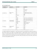
Table 17 BOOTMODE Description
BOOTMODE pins
Description
Pin Settings
Pin Behavior
BOOTMODE[15:14]
Reserved by the processor
XX
None
BOOTMODE[13:10]
Backup boot mode
selection
X000
None
0001
USB device mode
1001
USB host mode
X011
UART
0100
Ethernet RGMII with internal TX delay
1100
Ethernet RMII with external clock source
0101
MMC0
1101 (Default)
MMC1
X110
SPI
X111
I
2
C
BOOTMODE[6:3]
Primary boot mode
selection and config
X00_0001
OSPI boot, Iclock is external, Boot flash is off
X01_0001
OSPI boot, Iclock is internal, Boot flash is off
X10_0001
OSPI boot, Iclock is external, Boot flash is on
X11_0001
OSPI boot, Iclock is internal, Boot flash is oon
XXX_1001 (Default)
eMMC boot
1X0_1000
SDIO boot in filesystem mode
1X1_1000
SDIO boot in raw mode
BOOTMODE[2:0]
PLL Reference Clock
selection
000
19.2 MHz
001
20 MHz
010
24 MHz
011 (Default)
25 MHz
100
26 MHz
101
27 MHz
1
:
X means the pin is reserved by the processor and must be tied either high or low. The direction doesn’t matter as long as the pin is not left floating.
To modify the default boot configuration on a custom carrier board, it is recommended to use 1k
Ω
pull-up resistors to
VDD_3V3_OUT (found on pins B1/B2 at the phyCORE-Connector) or 10k
Ω
pull-down resistors to override the SOM
settings. For startup/verification testing, PHYTEC recommends designing the boot configuration circuit to include a DIP
switch. This will make it easy to swap between various boot modes (an example circuit is shown below). This DIP switch
can then be de-populated for production.


