PCM-072/phyCORE-AM64xx System on Module
L-860e.A0
© PHYTEC America L.L.C. 2022
54
•
Avoid any cuts in the ground plane or other references planes within the RGMII routing region.
•
Place termination resistors (recommended to use 22Ω) near the PHY on
all the RGMII RX* signals.
•
The MDIO clock and data signals do not need to be matched as strictly as RGMII. However, it is recommended to
route these together and keep them length matched within 2540 µm.
•
RGMII v2.0 Timing Requirements (shown in the table below) specify that the clock and data will be generated
simultaneously by the transmitting source, which requires a skew be introduced between clock and data.
Table 23 phyCORE-AM64xx RGMII Timing Requirements
Parameter
Minimum
Typical
Maximum
Units
Data to clock output skew at transmitter
-500
0
500
ps
Data to clock output skew at receiver
1
1.8
2.6
ns
The skew can be introduced with additional PCB trace delay added to the clock signal on the carrier board or by adjusting
the internal delay settings at the PHY or processor. However, please note that an internal delay may not be available on
your selected ethernet PHY or it may not have sufficient adjustment to account for the required skew. The skew between
the clock and each individual data and control signal should not fall below the 1ns minimum or exceed the 2.6ns maximum.
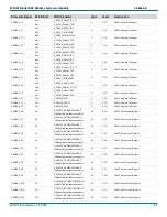
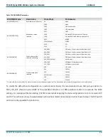
Ensure signals are properly length matched to meet these RGMII timing specifications. The following tables show the signal
groups (TX vs. RX) that should be length matched and the trace length of each signal on the SOM. It is recommended to
length match the control and data signals within 2540 µm, and then the trace length of the clock should be the average
length of these control and data signals plus an additional 1.8ns delay. The recommended clock trace length on a carrier
board is calculated using the following equation:
(Average total length of control/data signals on SOM) + (Average total length of control/data signals on Carrier Board) +
(1.8ns delay) – (Clock Trace Length on the SOM)
An example of using this equation to calculate the recommended clock lengths when implementing a physical delay for
PRG0_RGMII1 is shown in the equations below. The 1.8ns was translated to an estimated length using the general rule of
6.5ps/mm. However, the actual physical trace delay will vary depending on the PCB stackup, materials, etc.
•
Transmit Clock Length Calculation with Physical Trace Delay: (17386 µm) + (Average total length of control/data
signals on Carrier Board) + (276860 µm) – (17196 µm)
•
Receive Clock Length Calculation with Physical Trace Delay: (20030 µm) + (Average total length of control/data
signals on Carrier Board) + (276860 µm) – (19732 µm)


