Commissioning
Operating Manual PNOZ ml1p
21575-EN-06
19
6.4
Connection examples
6.4.1
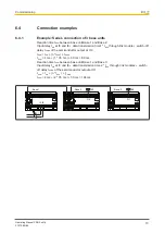
Example: Series connection of 3 base units
Reaction time t
SUM
between base unit Base 1 and Base 2:
Input delay t
ON
at I3 and I6 + data transmission time1 * t
BUS
through link switch-off
delay t
COND
of the semiconductor output at O0
t
SUM
= t
ON
+ (n * t
BUS
) + t
COND
t
SUM
= 4 ms + (1 * 35 ms ) + 30 ms = 69 ms
Reaction time t
SUM
between base unit Base 1 and Base 3:
Input delay t
ON
at I3 und I6 + data transmission time 2 * t
BUS
through link m switch-
off delay t
COND
of the semiconductor output at O1
t
SUM
= t
ON
+ (n * t
BUS
) + t
COND
t
SUM
= 4 ms + (2 * 35 ms ) + 30 ms = 104 ms
CHIP-Card
Shield
CHIP-Card
CHIP-Card
Shield
Shield
Shield
S1
K2
K3
I3 I6
O0
O1
Base 1
Base 2
Base 3


