61
PDP-5020FD
5
6
7
8
5
6
7
8
A
B
C
D
E
F
Is the function correspondeing to
selected signal input selected?
Select the corresponding signal
with the Input selector.
No
Check the 40P FFC (J214) between MAIN Assy and
IO Assy. If there was problem, replace it.
No
Check around IC8001 and check the communications
between IC8001 and microcomuputer.
If there was no ploblem, replace the IO Assy.
No
No
No
Check around the input terminals.
No
Replace the IO Assy.
NG
Yes
Yes
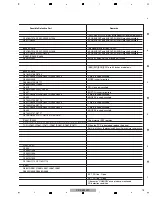
Image for the composite or S-video
signal is not displayed.
=> COMP/S1
Has the signal arrived at IC8001?
(AVSW)
Which signal is not output,
main or sub signal?
Is a signal output from IC8001?
(AVSW) (pins 42, 45)
Yes
Has the signal arrived at IC4702?
(VDEC) (pins 22, 26)
Yes
Has the signal arrived at IC4702?
(pins 69, 70)
Yes
Yes
Yes
MAIN
SUB
7
6
9
11
Is a signal output from IC8001?
(pins 47, 49)
13
12
15
14
8
10
6
IC8001 - pin 68 (Y)
V: 500 mV/div H: 20
μ
sec/div
7
IC8001 - pin 70 (C)
V: 500 mV/div H: 20
μ
sec/div
8
IC8001 - pin 45 (Main Y)
V: 500 mV/div H: 20
μ
sec/div
9
10
IC8001 - pin 42 (Main C)
V: 500 mV/div H: 20
μ
sec/div
IC4702 - pin 22 (Main Y)
V: 500 mV/div H: 20
μ
sec/div
11
IC4702 - pin 26 (Main C)
V: 500 mV/div H: 20
μ
sec/div
12
IC8001 - pin 49 (Sub Y)
V: 500 mV/div H: 20
μ
sec/div
13
14
IC8001 - pin 47 (Sub C)
V: 500 mV/div H: 20
μ
sec/div
IC4702 - pin 70 (Sub Y)
V: 500 mV/div H: 20
μ
sec/div
15
IC4702 - pin 69 (Sub C)
V: 500 mV/div H: 20
μ
sec/div
Waveforms
Input signal: NTSC Color-bar (S termial)
Check around the IC that is found to have failure in
communication and the microcomputer.
If there was no ploblem, replace the MAIN Assy.
No
Replace the MAIN Assy.
Yes
Yes
Is the communication between
each IC (VDEC, ASIC) on the
MAIN Assy and the microcomputer
normal?
No
Specifications that does not
display in the sub-side.
Is the screen of main side Tuner?
Summary of Contents for ARP3476
Page 10: ...10 PDP 5020FD 1 2 3 4 A B C D E F 1 2 3 4 2 2 SPECIFICATIONS ...
Page 11: ...11 PDP 5020FD 5 6 7 8 5 6 7 8 A B C D E F ...
Page 12: ...12 PDP 5020FD 1 2 3 4 A B C D E F 1 2 3 4 2 3 PANEL FACILITIES Front Section ...
Page 13: ...13 PDP 5020FD 5 6 7 8 5 6 7 8 A B C D E F Rear Section ...
Page 14: ...14 PDP 5020FD 1 2 3 4 A B C D E F 1 2 3 4 Remote Control Unit ...
Page 15: ...15 PDP 5020FD 5 6 7 8 5 6 7 8 A B C D E F ...
Page 21: ...21 PDP 5020FD 5 6 7 8 5 6 7 8 A B C D E F ...
Page 22: ...22 PDP 5020FD 1 2 3 4 A B C D E F 1 2 3 4 4 BLOCK DIAGRAM 4 1 OVERALL WIRING DIAGRAM 1 2 ...
Page 25: ...25 PDP 5020FD 5 6 7 8 5 6 7 8 A B C D E F OVERALL DIAGRAM PDP 5020FD ...
Page 31: ...31 PDP 5020FD 5 6 7 8 5 6 7 8 A B C D E F ...
Page 71: ...71 PDP 5020FD 5 6 7 8 5 6 7 8 A B C D E F ...
Page 192: ...192 PDP 5020FD 1 2 3 4 A B C D E F 1 2 3 4 9 6 PANEL CHASSIS SECTION ...


