background image

47

AVIC-W8400NEX/XNUC

5

6

7

8

5

6

7

8

A

B

C

D

E

F

6. SERVICE MODE

6.1  TEST MODE

Allocation of Key Operation

1. Start the product and wait until the map is displayed.
2. Press "Vol+", "Vol-", "Vol+" and "Vol-" in that order.
3. While pressing "      (MODE)", press "      (MENU)" twice and "     (HOME)" twice.
4. Release "      (MODE)".
5. Press and release "      (MODE)".
6. Product restart starts automatically, and it displayed the Test Mode Main Menu.

* The underlined blue texts are linked to detail description page.


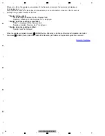
: Selection cursor up

VOLUME-  


: Selection cursor down

(Long press)   : Page change (next page)
VOLUME- (Long press)  

: Page change (previous page)

     (HOME)  


: Enter the selected item

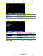
Test Mode Menu Item

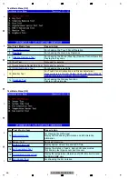
Test Mode Menu [1/5]

[How to enter Service Test Mode]

[Test Mode Menu]

T e s t M o d e I t e m

D e s c r i p t i o n

Clear Sensor Learning Data

Display software version of each program.
This item can check communication between SOC and
each device.

Not used for service

For re-writing program

Not used for service

Clear Application User Data and Bluetooth Settings

5

6

N o .

Clear Sensor Data

1

2

3

4

Version Information

Write Program Forcedly

Error History

File Maintenance

User Setting Initialize

* The time to judge that VOLUME button is long pressed is about 1 second. (Each item is the same)

Summary of Contents for AVIC-W8400NEX/XNUC

Page 1: ... Kilang Barat 07 01 Singapore 159346 PIONEER CORPORATION 2018 AVIC W8400NEX XNUC CRT6189 MULTIMEDIA NAVIGATION RECEIVER AVIC W8400NEX XNUC NAVIGATION AV SYSTEM AVIC Z910DAB XNEU5 AVIC Z910DAB XNAU AVIC Z810DAB XNEU5 This service manual should be used together with the following manual s Model No Order No Mecha Module Remarks CX 3311 CRT5651 LS2 5 DVD Mecha Module Circuit Descriptions Mecha Descrip...

Page 2: ...r WARNING The AEL accessible emission level of the laser power output is less than CLASS 1 but the laser component is capable of emitting radiation exceeding the limit for CLASS 1 A specially instructed person should do servicing operation of the apparatus CAUTION This product is a class 1 laser product classi fied under the Safety of laser products IEC 60825 1 2007 and contains a class 1M laser m...

Page 3: ...NSPECTION METHOD OF PICKUP UNIT 34 5 9 ERROR CODE LIST 37 5 10 CLEAR CONDITION AND LOCATION OF PROGRAM SYSTEM SETTING VALUE ETC 39 5 11 CONNECTOR FUNCTION DESCRIPTION 45 6 SERVICE MODE 47 6 1 TEST MODE 47 6 2 DVD TEST MODE 81 7 DISASSEMBLY 86 8 EACH SETTING AND ADJUSTMENT 97 8 1 ADJUSTMENT REQUIRED WHEN THE UNIT IS REPLACED 97 8 2 FLICKER ADJUSTMENT 98 8 3 CALIBRATION ADJUSTMENT AVIC W8400NEX AVIC...

Page 4: ...DMI MHL RX A B C 156 10 40 SERVICE IF UNIT 1SEG_IF 157 10 41 SERVICE IF UNIT LS2 5_IF 158 10 42 SERVICE IF UNIT M_CHIPS IF 159 10 43 SERVICE IF UNIT ECHO CANCELLER 160 10 44 SERVICE IF UNIT MIC ADC 161 10 45 SERVICE IF UNIT AUDIO SEL I2S 162 10 46 SERVICE IF UNIT DAC 163 10 47 SERVICE IF UNIT MONITOR_IF 164 10 48 SERVICE IF UNIT 1F 2F_IF 164 10 49 SERVICE IF UNIT USB_IF 166 10 50 SERVICE IF UNIT I...

Page 5: ... pickup and make adjustment and do not look straight at Laser Beam for more than 10 seconds area and a heat sink becomes hot areas Be careful not to burn yourself Heat Sink DVD Mechanism Module Top Case IC9201 IC201 Before disassembling the unit be sure to turn off the power Unplugging and plugging the connectors during power on mode may damage the ICs inside the unit To protect the pickup unit fr...

Page 6: ...crocomputer changes to L BUP OFF processing starts The RESET pin 16 pin changes to L Hardware reset Forced reset by RESET pin Section 2 is necessary for resetting when the microcomputer becomes abnormal deadlock state and it has a circuit Circuit diagram of hard key reset Lo RST DB2J31400 Lo KEY_RST DB2J31400 PVDD3 3u RST IC KEYRST Circuit Connector ucom 16 RESET 152 KEY_RST Buffer PVDD3 3u 18k 22...

Page 7: ...EYBOARD UNIT replace KEYBOARD UNIT AVIC Z810DAB XNEU5 Because difference occurs in brightness Unit AV UNIT SERVICE IF UNIT SOC UNIT MONITOR UNIT Ref No Part No Reason IC801 IC8401 IC8401 IC8551 TEF6686HN V102 Heat pad IC9001 IC4801 IC5851 IC5852 IC3952 IC4401 IC4002 CN9801 IC6901 IC7201 IC7202 IC7301 IC7302 U7701 IC6703 IC6701 IC7501 CN7901 IC7401 IC5201 IC5101 LV2241PQA TEF6688HN V102 PM9015A IT6...

Page 8: ... the backup current refer to the Owner s Manual 2 5 mA or less is a trademark of DVD Format Logo Licensing Corporation The Bluetooth word mark and logos are registered trademarks owned by the Bluetooth SIG Inc and any use of such marks by PIONEER CORPORATION is under license Other trademarks and trade names are those of their respective owners ...

Page 9: ...y back a CD Track search CD 6 Display audio and operations must be normal Check FM AM Tuner action Seek Preset Switch band to check both FM and AM FM AM Tuner 7 Display video audio and operations must be normal Check USB memory action Seek Preset USB 8 Current location must be correct Display and operations must be normal Connect GPS antenna to the product and check whether the current location is...

Page 10: ...ber CWF1716 A Unit Number CWF1717 B C D Unit Name SOC Unit Unit Number CWF1715 Unit Name DVD Core Unit Unit Number CWX4717 Unit Name Service IF Unit Unit Number CXY1372 A Unit Number CXY1373 B Unit Number CXY1374 C Unit Number CXY1375 D Unit Name Service ANT Unit Unit Number CXY1389 Unit Name CHIPS B COMP Unit Unit Number CWX4951 Unit Name Monitor Unit Unit Number CWF1751 A B C Unit Number CWF1752...

Page 11: ...NIT DVD MECHANISM MODULE LS2 5 Jigs List Name Jig No Remarks Grease GEM1024 DVD Mechanism Module Drive Unit Grease GEM1045 DVD Mechanism Module Grease GEM1043 DVD Mechanism Module Drive Unit Grease List Before shipping out the product be sure to clean the following portions by using the prescribed cleaning tools Portions to be cleaned Cleaning tools DVD pickup lense Cleaning liquid GEM1004 Cleanin...

Page 12: ...XNEU5 C AVIC Z910DAB XNAU D AVIC Z810DAB XNEU5 Note When ordering service parts be sure to refer to EXPLODED VIEWS AND PARTS LIST or ELECTRICAL PARTS LIST 4 BLOCK DIAGRAM EXTERNAL IF 18 18 A RGB IF 17 18 A INTERNAL IF 16 18 A AEQ 15 18 A MIC FILTER 14 18 A FLAP_MECHA 13 18 A WWR 12 18 A M_LITHIO TMC 11 18 A M_LITHIO FMAM 10 18 A FMAM DISTRIBUTION 9 18 A S_HIOUT AMP 8 18 A DUAL ZONE 7 18 A M_E VOL ...

Page 13: ... 30pin FFC MIC JACK from RGB CONNECTOR IC801 LV2241PQA from SoC Debug Chip Antenna BT WIRED REMOTE INPUT WIRED1 WIRED2 ANI11 12 INDP8L R DVD Mechanism Module Separate the iPhone and the Android to AVSEL 20pin FFC For Hardware SPEED PULSE IC103 NJM12904V AU8A IC301 NJW4184DL3 08A MIC5 IC311 MM1856A50N MIC FILTER IC1051 NJM4580V IC8401 IC8551 MIC IN IC2301 ACC5 ACC5 ACC5 WWRD12 IC310 S 1172B12 E6 WW...

Page 14: ...IC2502 74LCX157FT ADC IC2401 AK5720VT HDMI Rx IC4801 IT68013FN I2S SEL F1 IC2501 74LCX157FT S PDIF USB2 CDP SXi mono EVOL_CLK EVOL_CS EVOL_DI EVOL_DO FAUDIO_MUTE RAUDIO_MUTE GUIDE_MUTE HDMIRX_MUTE HDMIRX_DEEM I2SSELR0 I2SSEL1 HIOUTCLK AIN1L AOUT1L AOUT2L AIN2L L MCLK BCK LRCK BCK LRCK REARMUTE BUP OFFSET AMPMUTE I2S Analog voice Other signals Exclusion Source not covered by DualZone Rear output Ou...

Page 15: ...C_RS FV_I2C LPF ISO HiZ 75ohm 75ohm 75ohm 75ohm HiZ LoZ ISO 75ohm 150ohm Emitter follower buffer 75ohm CDP IC5851 MAX14644ETACNE USB SLOT1 USB SLOT2 HDMI MHL HDMI MHL Rx IC4801 IT68013FN HDR_I HDR_RST HDR_RQ 75ohm ISO Emitter follower buffer HiZ VCR Back Camera AUX USB 2port RGB26 Emitter follower buffer SD image quality BT656 8bit 480p 54MHz SD image quality BT656 8bit 480i 27MHz IC6901 MCIMX6D6A...

Page 16: ... UC TEF6688HN V102 EU AU TEF6686HN V102 RDS TMC TUNER TEF6686HN V102 3137 1015 2111 4194 6pcs Current 9061 44mA BUPV to NAVI 0 93W 200 0 34W 200 1 23W 0 56W 9766 5572 9 57W D D converter IC201 AN33012UA ACC8 ACCPW DDCLK_S ACC5 to NAVI 0 003 1777 ACC8 to NAVI 383 0 40W 126 175 MIC AMP IC1051 NJM4580V 9 Tr LSCR523UB ACC5 AU2 8 0 5 Reg MM1856A50N ACC8 9 5 0 5 9 5 5572mA 0 003mA 1015mA 0mA 7 2mA 1777m...

Page 17: ...M9015A 140 0 31W 3 3 Reg IC305 NJM2886DL3 33 SYSPW 95 6ch Line AMP IC701 NJW1240V 20 PWR AMP circuit Around OFFMUTE 0 91 0 45W 5 78 Reg MM1856A58N OPPW Tr 2SCR573DG MOTPW2 85 3 PWR AMP IC9201 TCB501HQ 800 0 61W AVSEL IC501 AK4223VQ 50 BUP14 4 to NAVI 690 0 39W MAX 0 32W MAX With diode 100 1000 500 1000 7 2 7 7 8 2 High voltage 6 5 7 Normal Rating Thermal resistance Limit 179 W 0 7W 0 36W 90 140 4 ...

Page 18: ...le mA Loss 41 60 0 01 1000 Since the power supply is supplied from the internal LDO of SoC it is added to the current value of each original power supply Refer to the left for the connection destination 3 3 3 3V 1 425 5893 3653 3 3 4093 2209 1636 489 Remarks 3 3 5162 3736 5162 Voltage value V Power supply name Current value mA 27 4 1228 1636 50 80 13 8 1543 3736 3 3 264 560 5V power supply IC3901 ...

Page 19: ...416EBLL45 SRAM 1 1 8 16 3 7 5 2 4 200 16 0 400 53 36 8 VCXO FPGA1 2 Reg IC6708 MM3479A12P Reg IC6712 MM3411A18N Echo canceller IC2301 AK7738VQ FPGA IC7501 PE1039A ICE40HX8K iPod CPIC mA mW CCPW VCC 1 62 3 3 5 5 7 5 VDD 3 3 3 3 6 1 8 VCC 1 14 1 2 1 26 36 75 VCC 2 2 3 3 6 6 12 0 03 0 165 On standby VCCIO 1 71 3 3 3 46 16 29 TVDD 1 7 3 3 3 6 1 6 2 4 Other power supply is on Service IF Unit side SD re...

Page 20: ...WVDD3 3 to AV ACC5 from AV 7 0 2 AU8 4 form AV ACC8 from AV 1777 7 2 1015 0 0028 5417 CCD5 from AV 0 FET SW RZQ050P01 CCPW 430 1 14 Tr LSCR523UB ADA5 82 5 2 4W 52 1 W 1 25W 63 585 190 690 Reg MM1856A50N ACC8 Echo canceller Analog input line ISO NJM2740V Echo canceller DAC Filter NJM2740V 5 1 5 14 17 SWVDD3 3 to AV 0 003 17 1 17 5 Echo canceller ADC Filter NJM2740V MIC AMP NJU7043V Speech recogniti...

Page 21: ...T 60 3000 1765 0 033 602 086 1112 D D converter MM3630BR DDEN DDCLK_U LSAR523UB ACCPW I2S SEL x 2 CCD3 3 to Monitor ILM8 to Monitor 329 0 ohm ACC5 to Monitor SiriusXM Tuner SXI CAN 3 3 5 converter 1 5 0 02 iPod USB To power supply microcomputer For Bup voltage indication 5 25 5 2 7 27 27 5 5 5 4 5 70 45 5 0 033 0 033 16 13 8 10 2 0 033 0 033 5 25 5 4 75 1500 USB55 5 25 5 4 75 1500 5 25 5 4 75 3000...

Page 22: ...D No retention UHS compatible TEMP33 To CC internal HDMI Rx IC4801 IT68013FN 72 SACC33 To CC internal CCD33 To CC internal 2c NACC3 3 SD_PEN ACCPW CCD3 3 CCPW DDCLK_S 4150 1 5445 0 317 3725 0 017 1636 413 200 Tr SW 2SB1689 UHS2_ERR2 UHS_EN FET SW RZQ050P01 ACCPW 5162 5162 0 ohm Buffer circuit for CHIPS CHIPS 317 MEDIA SD Holded UHS not supported Tr SW 2SB1689 SDPEN 152 3 6 3 3 1 4 0 017 3 6 3 3 3 ...

Page 23: ... 3 Total of CCD3 3 Speech recognition ADC IC2401 AK5720VT 7 VENC IC4502 AK8814VQ 65 255 Echo canceller IC2301 AK7738VQ 190 T CON IC4701 ML86287 172 USB re driver IC5852 TUSB211QRWBQ1 20 3 6 3 3 3 255 1 65 1 5 1 35 172 3 6 3 3 3 190 86 5 5 3 3 2 7 7 4 4 3 6 3 65 50 3 6 3 3 3 20 16 3 45 3 3 3 2 3023 9 2260 7 8 9 CCD3 3 VDEC1 5 ...

Page 24: ... 10 6V COMDC NJM8065RB1 Touch Panel Clear Resistive CSX1241 Reg MM3411A33N Stand by max 50 35 50 35 1 0 5 max 100 LCD current value max typ min 1 5 max To SERVICE IF UNIT max 60mA Dual Touch IC5001 AK4187VN typ 275mA max 275mA NSSM124 6717 x5 R max 15 3mA G B Remote IC U6001 RS 470 max 19 9mA max 19 9mA max typ min max typ 5 5 3 3 2 7 1 5 1 2 RS 470 max 2mA max 275 2mA Parameter Symbol Min Typ Max...

Page 25: ...n AMP Error is displayed on this manual When Power AMP is defective this error will not be displayed AV unit Product overheat System will be shut down automatically in 1minute is displayed Try to restart the unit by ACC Off On If not solved check the check points on this manual This error is displayed when SOC temperature is more than 95 degrees C Refer to Diagnosis when Product overheat is displa...

Page 26: ...mperature sensor or ADC Check the installation angle and direction then reset 3D Learning status Check External Connection Test in Test mode If the sensor check is NG replace CHIPS B COMP Unit CHIPS B COMP Unit Detected changes in the installation angle or position Head unit is updating the sensor learning data This message appears when the installation angle or position changing is detected The u...

Page 27: ...UART CHIPS SOC R7512 R7511 IC7501 FPGA R9502 CCD3 3 IC9651 uCOM SPEED PULSE R9518 0 10k SENSOR SPEED PULSE 10k 100 0 0 470 470 0 ACC5 C114 0 1u 16 C119 0 1u 10 C116 NM C115 0 01u 16 C118 1000p 50 C117 0 1u 16 D116 DA2J101 D118 DA2J101 D117 NM GNDD GNDD GNDD IC103 NJM12904V 3 4 GND 2 1 8 VCC IC103 NJM12904V 5 6 7 LTC014EEB Q110 LTC014EEB Q111 R143 2k R149 51k R151 56k R147 51k R141 51k R158 100k R1...

Page 28: ...ror SOC_OFF_RDY Starts communication with SOC Source keys Source ON BSENS6 H ASENS L DVD Status is Normal SOC Temperature is Normal SOC is Ready Power ON Completes power on operation After that proceed to each source operation ASENBO H Pin 58 SOC_RST H Pin 131 Pin 90 SYSPW H Pin 140 AMPPW H Pin 56 Signal on System ucom IC4002 ...

Page 29: ...13 C1214 C8551 C8552 C8553 C8555 C8556 L8412 L8413 C8557 C8558 L8414 C8559 L8415 R505 L8416 R506 JA101 R123 C8560 R124 C8561 R125 Q9309 C8562 C8565 CN301 C8566 VL8402 R130 R131 R132 R133 R906 R907 R1210 D8551 R1211 R1212 C8577 R1408 R8551 C101 R1409 C102 C103 R9301 P201 R9302 R8557 R8558 C108 R1410 IC8551 R8559 R1411 C1052 C8583 C1053 C1054 R919 Q1051 C1055 C1056 R1417 R8560 R1418 CN901 C1059 R141...

Page 30: ...V DC DC converter of AV UNIT POWER ON ACC OFF ON Failure of Flexible Cable and Connector between SERVICE IF UNIT and MONITOR UNIT Is the Backlight Cable of TFT LCD connected correctly Failure of Flexible Cable and Connector between TFT LCD and MONITOR UNIT IC5101 failure TFT LCD failure IC201 NACC8 DC DC P201 L201 K Bup IC5101 BackLight POWER IC CP1 CP2 D5101 CP3 CP4 Implementation failure of Resi...

Page 31: ... AV UNIT Side A 8 V Confirm that the CP2 L201 AV UNIT is 8 V Confirm that the CP3 D5101 cathode MONITOR UNIT is 18 6 V 2 V MONITOR UNIT Side A 18 6 V 2 V MONITOR UNIT Side A 3 3 V 3 3 V Confirm that CP4 Pin10 and Pin22 of IC5101 MONITOR UNIT are 3 3 V ...

Page 32: ...ure DVD mecha pickup Temperature 60 degrees C or more 70 degrees C or more 79 degrees C or more 74 degrees C or less Rotation Control SLOW FAST STOP SLOW MEDIUM FAST MEDIUM MEDIUM 62 degrees C or less 50 degrees C or less SLOW MEDIUM SLOW STOP SOC Thermistor Temperature 40 degrees C or more 60 degrees C or more 90 degrees C or more 81 degrees C or less 55 degrees C or less 35 degrees C or less The...

Page 33: ...t with the other patterns Confirm that SYSCON Pin 142 is DC3 3V when voice is turned off If not so confirm that R4296 is incorrectly mounted and the OFFSET signal line is not short circuited with the other parts and patterns Point to be checked when Product Overheat is displayed 1 Confirm that the following parts are mounted on the SOC Unit correctly R7207 R7208 TH7201 2 Confirm voltage of the fol...

Page 34: ...V1025 Exact judgment cannot be performed if the disc to be used has a crack and dirt Be careful of handling of a disc enough Execution method Refer to next page for the details of the check 1 and the check 2 PU Lighting Please perform the usual diagnosis No Is it OK PICK UP cleaned Perform lens cleaning Error rate check Replace the DVD mecha module Yes Yes Yes Yes Yes No No No No No Replace the DV...

Page 35: ...f TEST MODE Notes Please pay attention to the laser diode damage by static electricity Check Point DVDLD1 VCC5_PU No 1 Disc GGV1025 Remarks LD current 10 65 mA Threshold 120 780 mV CDLD1 VCC5_PU 2 TCD 782 10 60 mA 150 900 mV Check Point No Disc Remarks LD current Threshold DVDLD1 VCC5_PU CDLD1 VCC5_PU ...

Page 36: ...ue of ASMAX on display No 1 Disc GGV1025 Remarks Threshold More than 0000 0B00 2 TCD 782 More than 0000 0E00 Check2 Error rate check Check Status Tracking Closed of TEST MODE ID 40000 1 GGV1025 Less than 1 000E 3 2 GGV1025 3 TCD 782 ID 200000 Less than 1 000E 3 ID HOME Position Less than 2 500E 3 8 digits value of ASMAX on display Check Point No Disc Remarks Threshold ...

Page 37: ...rted by this product Overcurrent Error Pandora Error Code Message Description ERROR 02 ERROR 03 ERROR 14 Boot Error of the Bluetooth Module Fatal Error after boot Required Bluetooth Module Reset BT Service abnormality shut down Bluetooth USB SD Error Code Message Description Unplayable File Incompatible USB Incompatible SD Check USB Unplayable File Incompatible USB Incompatible SD Overcurrent Erro...

Page 38: ...re is 89 C or higher Read Error Transfer Start Error Focus Error Focus Error during set up Focus has never been achieved with that disc Address not found Invalid Track Spindle lock NG Disc cannot be rotated Carriage home NG Pick up tries to return to carriage home but it cannot go back and stopped ID SUBCODE Read Error ID SUBCODE cannot be read due to scratch or stain AV CHIP decode NG AV chip can...

Page 39: ...WITH A DIFFERENT 3 AND ERASE IT when transitioning to the ARM screen p 7HEN THE PRESET MEMORY CAPACITY IS OVER ICONS delete the last History App icon in the sort order App icon sorting order Soc When the History App forgetting condition is satisfied except the default memory capacity over Customize Favorites on the HOME menu Soc Both the AV area and the Device area Do not show again Device selecti...

Page 40: ...n CHAPTER REPEAT state CHAPTER UP DOWN p 4 4 50 7 p 2 6 p 3 4 X X X iPod Device Depends on iPod REPEAT X Sys No BOOKMARK BOOKMARK X X X X Sys Depends on disc Audio language switching X X X X Sys Depends on disc Subtitle language switching X X X X Sys Full 5 4 SWITCHING X X X X X REPEAT ALL DISC ALL Disc Sys USB SD SD p FOLDER UP DOWN p Selection of FILE from LIST including CURRENT FILE p HANGE HAN...

Page 41: ...ing value is managed on the external device side The setting value is managed on the external device side The setting value is managed on the external device side The setting value is managed on the external device side The setting value is managed on the external device side SHUFFLE Depends on iPod iPod Device AUDIO BOOK Speed setting Depends on iPod iPod Device Change Operating Bar Display Timeb...

Page 42: ... X X X X X X X X X X X X X X X X X X X X X TIME ALIGNMENT STEP Sys X X X CUTOFF frequency Sys X X X SD X X X OFF BASS BOOST Sys X X X 0 Sound Setting Save data Sys X X X LOUDNESS Sys X X X OFF POSITION Sys X X X X All Seats GRAPHIC EQ PRESET setting Sys X X X GRAPHIC EQ fine adjustment Sys X X X ASL Sys X X X OFF Tuning exclusively for car models ON OFF Sys X X X X ATT Mute level setting Sys X X N...

Page 43: ...r Photo Slide Sys X X X X Trip meter Chips X 0 Vehicle speed pulse numbe Chips X Unlearned Sensor learning Chips X Unlearned Distance learning degree Chips X Unlearned Direction learning degree right Chips X Unlearned 3D learning degree Chips X Not Registration DivX VOD Mecha It is necessary to initialize after deleting the registration Because of the specification of the authentication request it...

Page 44: ...e Dimmer value can be initialized History App Icon has a restriction that Icon is not saved when it is B UP during saving When upgrading the version Source Mode switches to OFF but the inside is not initialized Condition for initializing setting value Remarks Return to the factory shipment state Normal Other initialization conditions Category Setting Initial value Storage location A OFF B UP RESET...

Page 45: ... 16 4 17 5 18 6 19 7 20 8 21 9 22 10 23 11 24 12 25 13 26 GNDAU NC GNDD NC NC NC terminal name DSEN NC MXTOEX terminal name CCAUR NC NC EXTOMX HYOKA NC NC NC NC NC GNDSIG NC NC NC CCAUL NC NC 26 24 22 20 18 16 14 12 10 8 6 4 2 25 23 21 19 17 15 13 11 9 7 5 3 1 1 2 3 4 5 6 7 8 9 10 11 12 13 14 15 16 17 18 10A FUSE A B 1 3 5 7 2 4 6 8 9 10 11 12 13 14 15 16 17 18 RL RR RL REV GND BUP PKB RR ACC BREM...

Page 46: ...LOCK GND NC CEC GND 5V DATA2 DATA0 CLOCK DATA1 GND CEC NC DDCSCL DDCSDA 4 3 2 1 5 7 9 11 13 15 17 19 6 8 10 12 14 16 18 1 2 3 4 5 6 7 8 9 10 1 2 3 1 2 3 4 C D E F 1 2 3 4 2 1 4 3 6 5 8 7 9 10 11 12 13 14 15 16 17 18 19 GNDE 4 3 2 1 1 2 3 4 GNDE GND GND terminal name USB5V USB D USB D AV CONNECTOR G 13 14 12 11 10 9 8 7 6 5 4 3 2 1 23 24 22 21 20 19 18 17 16 15 terminal name terminal name 1 13 2 14...

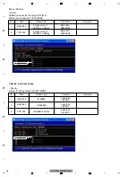
Page 47: ...wn VOLUME Long press Page change next page VOLUME Long press Page change previous page HOME Enter the selected item Test Mode Menu Item Test Mode Menu 1 5 How to enter Service Test Mode Test Mode Menu Test Mode Item Description Clear Sensor Learning Data Display software version of each program This item can check communication between SOC and each device Not used for service For re writing progra...

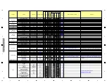
Page 48: ...ort Test Asynchronous Serial Port Test RGB Illumination Test Monitor Test Graphics Test 10 11 12 13 14 Test Mode Item Description Display the status of leads Gyro and G sensor value This item can test Gyro sensor and G sensor 19 Display the temperature information of SOC Monitor Unit and CHIPS B COMP Unit 20 For checking the Fan rotation Ext Connection Test Temperature Sensor Test Fan Control Test...

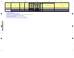
Page 49: ...iption Sensitivity check for OneSeg signal No applicable model HD Radio Data Test RDS TMC Test DTV OneSeg Test 29 For Re Writing Device Number UC model only 27 Not used for service 28 Audio Test for Production For checking the audio line Front Rear and Guide audio line can be tested Audio Test No 24 For checking the communication line between SOC and HD Radio Tuner UC model only 25 Sensitivity che...

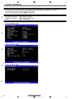
Page 50: ...ormation on screen This test mode item can be used for communication check When the communication is failed ERROR is displayed VOLUME Long press Page change next page VOLUME Long press Page change previous page BACK Return to Main Menu Outline Allocation of Key Operation Description Version Information 1 3 Version Information 2 3 Version Information 3 3 ...

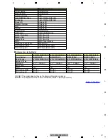
Page 51: ...em uCom SOC Flash ROM on SOC Unit Flash ROM on SOC Unit Storage SD Storage SD Storage SD Storage SD System uCom CHIPS B COMP Unit DVD Core Unit DVD Core Unit DVD Core Unit WWR Tuner Module Monitor Unit DTV Module NO_SET DTV Module NO_SET Information List by Model AVIC W8400NEX XNUC AVIC Z910DAB XNEU5 AVIC Z910DAB XNAU AVIC Z810BT XNEU5 Project Number NX450 XNUC NX450 XNEU5 NX450 XNAU NX451 XNEU5 M...

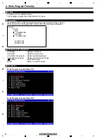
Page 52: ... writing is stored Make sure to store the program file in USB or SD in the following configuration Outline Preparation VOLUME Selection cursor up VOLUME Selection cursor down VOLUME Long press Media selection Next page VOLUME Long press Media selection Previous page HOME Enter Start writing BACK Return to previous screen Allocation of Key Operation Description Write Program Forcedly Menu 1 3 Write...

Page 53: ...ystem uCom Program can be written to System uCom 10 Write GPS Sensor Program can be written to GPS CHIPS B COMP Unit 11 Write 1seg Program can be written to One segment Module No applicable model 12 Write WWR Program can be written to WWR Tuner Unit 13 Write X 8116 DTV Program can be written to X 8116 DTV Module No applicable model 14 Write X 8116 Platform Data can be written to X 8116 Platform 15...

Page 54: ...pdate Failed is displayed If there is no file on the update source media or if the file name is incorrect the version is not displayed It is displayed as Also if you do not have all of the software to be updated you can not update it However if the file name is partially wrong update it except for that file Return to Top Menu When the update is completed press HOME button Rebooting is started and ...

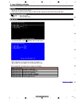
Page 55: ...nitialization press HOME button simultaneously When initialization is completed this screen is displayed Key operation is not accepted Turn off the power ACC OFF Details of Error Code ERRORCODE 0101 ERRORCODE 0102 ERRORCODE 0103 ERRORCODE 0104 ERRORCODE 0401 ERRORCODE 0402 Return to Top Menu Failed to BT initialization Failed to LiveInfo initialization Failed to Wifi initialization Failed to UserD...

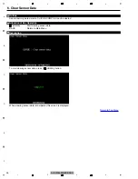
Page 56: ...Clear Sensor Data Sensor learning data stored in CHIPS B COMP Unit can be cleared BACK Return to Main Menu Outline Allocation of Key Operation Description To start clearing sensor data press HOME button When clearing sensor data is completed this screen is displayed Return to Top Menu ...

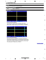
Page 57: ...ate is displayed as X1 Y1 at the bottom line on the screen X2 Y2 is fixed to 0 and the pushing status is displayed as PUSHED In case of two point touching The first touched point is displayed as a cross point of yellow lines The coordinate is displayed as X1 Y1 at the bottom line on the screen The second touched point is displayed as a cross point of pale blue lines The coordinate is displayed as ...

Page 58: ...n to Main Menu Outline Allocation of Key Operation Description Return to Top Menu KeyCode Status OFF WR IR U History The pressed key code is displayed ON Pressing the key Released the key Wired remote controller Infrared remote controller Other than the above remote controller Up to seven histories will be displayed ...

Page 59: ...n Allocation of Key Operation Description When a key on the steering remote control is pressed the key code corresponding to the key is displayed 1 Remote Control Key Test List of key codes of steering remote control 0x00000128 0x0000012b 0x00000123 0x0000012a BAND On Hook TEL OFF Off Hook TEL ON DISP 0x00000124 0x00000121 0x00000129 Cross Key Right RIGHT mode MODE Source PHONE 0x0000012c 0x000001...

Page 60: ... WIRED1 164 pin WIRED2 are displayed The range of the voltage value is 0 000 to 3 300 V 3 Learning Wired Remote Control Test Change the setting of WREMCONT1 WREMCONT2 to Hi Lo Hi Hi Lo Hi Lo Lo Use MODE button to switch between WREMONT1 and WREMONT2 Terminal name WREMCONT1 WREMCONT2 Initial value Hi Lo Cause of error Communication between microcomputer and SOC failed Learning type steering remote ...

Page 61: ...e VOLUME Selection cursor up and switches the key illumination color VOLUME Selection cursor down and switches the key illumination color BACK Return to Main Menu Allocation of Key Operation Description When selecting White R G B all color of LEDs Red Green Blue light on When selecting Red Green Blue each color of LED lights on Return to Top Menu ...

Page 62: ... It is an item for displaying 32 gradation grayscale bar 2 Color Bar Image It is an item for displaying the color bar 3 Plain Image It is an item for displaying the monotone screens 4 Flicker Adjustment Image It is an item for checking the flicker level of the screen 5 Cycle Line Image It is an item for checking the resolution function of the screen 6 10 Steps Image It is an item for displaying 11...

Page 63: ...n Image Pink Screen Plain Image Green Screen Plain Image Cyan Screen Plain Image Yellow Screen VOLUME Long press Screen change Allocation of Key Operation 3 Plain Image Plain Image Blue Screen Plain Image Red Screen 2 Color Bar Image Color Bar Image Screen ...

Page 64: ...ME Long press Screen change Allocation of Key Operation Flicker Vertical Stripe Screen Flicker Checkerboard Screen Flicker Horizontal Stripe Screen Flicker Mesh Screen Flicker Subpixel Lighting Screen Flicker Subpixel Lighting Screen Plain Image White Screen Plain Image Black Screen ...

Page 65: ...en 6 10 Steps Image 10 Steps Image Screen 7 Natural Image Displays an arbitrary image placed at a predetermined position of Media SD USB Reading priority of each media is as follows Return to Top Menu Priority 1 2 3 FilePath SD GraphicFile USB1 GraphicFile USB2 GraphicFile SD USB1 USB2 Media ...

Page 66: ... and Satellite Information are displayed GPS Information Sv Status 1 1 3 Sv Status 2 2 3 Ev C N0 Satellite azimuthal angle North 0 Clockwise plus Satellite elevation angle Signal level dB 3D 2D 0D T H Positioning dimension 3D 3D positioning 2D 2D positioning 0D No positioning Number of captured satellites Hdop V SV F Vdop Satellite number Positioning usage flag U Used Not used Azi On the 13th line...

Page 67: ...entation North 0 Clockwise plus Vertical velocity km h Long axis of error ellipse Not supported This value is fixed Short axis of error ellipse Not supported This value is fixed Angle of long axis of error ellipse Not supported This value is fixed Satellite number used for positioning Latitude Longitude Altitude m Horizontal velocity km h Return to Top Menu On the 13th line the meaning of the alph...

Page 68: ... uCom Time and GPS Time BACK Return to Main Menu Outline Allocation of Key Operation Description Time and Date are displayed Return to Top Menu NG code 001 002 003 004 Details of NG Invalid time data is input System time can not be acquired GPS time can not be acquired Time can not be set Error code list ...

Page 69: ...ation OK NG Information continues for more than 5 seconds the Variation is OK Display of Gyro Sensor Rotation Level Rotation angular velocity 50 0 Clockwise Rotation Level 3 Clockwise Rotation Level 2 Clockwise Rotation Level 1 No Rotation Counterclockwise Rotation Level 1 Counterclockwise Rotation Level 2 Counterclockwise Rotation Level 3 Sensor Output It displays the following values obtained fr...

Page 70: ...D value Determination of output value of Acceleration sensor 0x0 NG Other than 0x00 OK Variation It displays the following values obtained from sensor information for X axis Y axis and Z axis Acceleration sensor dispersion value Variation OK NG information 0x05 or 0x06 OK Other than those above NG Description Tilt angle 30 0 30 0 Tilt angle 20 0 20 0 Tilt angle 10 0 10 0 Tilt angle 20 0 20 0 Tilt ...

Page 71: ...d G Sensor Perform following procedure to check Gyro Sensor and G Sensor 1 Rotate the unit in clockwise and counterclockwise and Gyro Sensor detects 1 or more level in both of directions 2 Tilt the unit upward and downward and G Sensor detects 1 or more level in both of directions 3 Place the unit horizontally and do not move it for 5 seconds or more Return to Top Menu ...

Page 72: ... Mech Module Outline BACK Return to Main Menu Allocation of Key Operation Description When acquisition of temperature information is failed the following screen is displayed Communication Error Return to Top Menu Sensor SOC Unit Monitor Unit GPS Sensor DVD Mecha Module 40 to 125 C 20 to 125 C 40 to 125 C 13 to 101 C Temperature range Measurable temperature range DTV TEMP is not used ...

Page 73: ...he current status of FAN is displayed with green characters Press VOLUME Long press to switch between FAST MEDIUM SLOW and STOP When returning to Main Menu FAN control operation returns to the automatic control Regarding the automatic control refer to 5 6 FAN ROTATION CONTROL Return to Top Menu Outline Allocation of Key Operation Description Details of Error Code 1 2 Failed to switch FAN speed Fai...

Page 74: ...rsor up VOLUME Selection cursor down HOME Enter the selected item BACK Return to Main Menu Allocation of Key Operation Description 1 Media SD Test Write Read Test of SD Card in the SD Card Slot for user When HOME is pressed the inspection starts 2 Storage SD Test Write Read Test of Built in SD Card storing the product program When HOME is pressed the inspection starts When the inspection is comple...

Page 75: ... Hands free Microphone to MIC INPUT Preparation BACK Return to Main Menu Allocation of Key Operation Description Return to Top Menu Check the signal route from MIC input to speaker output during displaying this screen Error codes and error contents are listed in the table below Error code Contents of error BT Power ON error BT Loopback setting error Get BT Module Adpter error Change Source error 1...

Page 76: ...s not compatible with HD Radio HD Radio source can not turn ON Fail to request the test data transmission between SOC and Microcomputer Fail to request the test data transmission between Microcomputer and X 2069 Fail to request the test data transmission between X 2069 and SOC It can not confirm the correct test data within the specified time Request dummy data2 Request dummy data3 Data receive ch...

Page 77: ...r limit 108 0 MHz Can not select on UC model e Preset E Lower limit 87 5 MHz Can not select on UC model Values of Preset A to C correspond to Toyota standard analog radio specification 25 RDS TMC Test This test is for checking the reception sensitivity of RDS TMC at the specified frequency Outline Connect the antenna to receive RDS Preparation Description Allocation of Key Operation HOME Enter Sen...

Page 78: ...received data blocks Corrected Blocks Number of bit corrected data blocks Error Blocks Number of uncorrectable data blocks Return to Top Menu The cause is displayed if an error occurs during inspection Contents of error Error code 1 2 3 4 5 6 Fail to initialize Fail to request frequency setting No response to frequency setting request Failed to request error measurement start Error measurement res...

Page 79: ...is output from the rear sound line AUDMUX6 and from the guide sound line ESAI 1 Rear Audio Line Test Sine wave is output for the Rear audio line 2 Guide Audio Line Test Sine wave is output for the Guide audio line Details of Each Test Audio Test for Production Menu 1 Rear Audio Line Test Details SineWave 11kHz Sampling SineWave 22kHz Sampling Narration 11kHz Sampling Narration 22kHz Sampling Play ...

Page 80: ...r Contents of error Return to Top Menu Switching range VOLUME MUTE Play file switching can be performed during playback Selection item 0 to 31 OFF ON Error type Error code 1 2 3 4 5 Start playing error Volume setting error Mute OFF setting error Mute ON setting error MixData source setting error Contents of error 6 7 8 1kHz Sine Wave Audio File folder error 1kHz Sine Wave Audio File no found error...

Page 81: ...to allow implementation in the HOST communication The command for the test mode received in the HOST communication is interpreted by the application part converted to the PC communication command and transferred to the OS The OS transfers this command to the PC task as if it received the command in the PC communication The execution result is noticed to the application part by an e mail instead of...

Page 82: ...sed 1B00 0000 CRG 1C00 0000 CRG LD ON OFF When LO ON 1100 0000 When LD OFF 1000 0000 Power_OFF Disc type DVD2 layer Disc type CD 0000 0000 0100 0000 0200 0000 EJECT Disc type CD RW 0300 0000 F search STOP 1100 0000 0FFF 0000 1FFF 0000 CRG_HOME 1D00 0000 0X00 0000 Start of the test mode TEST FE test selection EDC1 test selection EDC2 test selection Hereafter to FE test mode image LD power on time m...

Page 83: ...acks 1 4 10 11 and 32 For DVD Tracks 1 4 10 11 32 64 and 100 Change the method for ID address designation Designation of digit by command 1 and 2 UP DOWN of numbers by command 3 and 4 Fix by command 5 8 Note If an error occurs at Power_OFF reset cannot be made In such a case it is necessary to turn the power off and start the test mode once again To 2 Error rate measurement Playback speed switchin...

Page 84: ...not be correct due to the life of the flash memory 1 4 EDC1 2 test mode 0000 0000 Layer 0 selection Layer 1 selection ID designation EDC1 2 start 0000 0000 0100 0000 1003 0000 1103 0000 Layer 1 11 Note is the ID designation value EJECT operation Test mode Eject LD power on time mode 0000 0000 CD LD power on time indication DVD LD power on time indication CD LD power on time setting 10 Note is the ...

Page 85: ... 1 DVD Single Layer 1 Inner Measurement 1 Power OFF 2 Outer Measurement 3 CD 3 Middle Measurement 5 Return 5 Return Error Rate 000000 Please Input Number Please Input Number Now Running Please Input Number 1 The position in which select was done is displayed Error Rate CD DVD Inner DVD Outer DVD Middle CD CD Error Rate CD Now Running CRG Move Outer CRG Move Outer CRG Move Outer 1 DVD Single Layer ...

Page 86: ...e the two screws and then remove the Monitor Assy 3 3 2 1 Monitor Assy Removing the Monitor Assy Fig 1 Method for opening the flap manually Insert a tip of screwdriver whose diameter is approximately 2mm into the slit at the bottom surface of the product and slide the flame part to the direction indicated by an arrow Mount the Collar for preventing Monitor Assy backlash on the red circle section C...

Page 87: ...installing DVD Mechanism Module please combine the bracket with DVD Mechanism Module and tighten the screw as shown below Make sure that the dowel of DVD Mechanism Module is in the slit of Bracket DVD Mechanism Module Bracket Don t remove this screws excluding the dismantlement of the DVD Mechanism Module Attention of removing Attention at assembly Attention at assembly a Hook on the left and righ...

Page 88: ...onnect the two connectors Straighten the tabs at two locations indicated Remove the two screws Disconnect the connector and then remove the Bracket 5 Bracket R Bracket L FRONT VIEW TOP VIEW LEFT SIDE VIEW RIGHT SIDE VIEW 5 4 4 3 3 1 1 2 Service ANT Unit Bracket Fig 5 Fig 6 Fig 7 Fig 9 6 Fig 8 6 Since it is difficult to work when assembling remove the connector only from the AV unit side ...

Page 89: ...l Jumper For inserting Coaxial Jumper adjust antenna cable with the engagement axis of connector and insert it as vertically as possible Do not insert the Coaxial Jumper in extreme slant as the connector might suffer damage Connector Coaxial Jumper GGF1539 Attach the bracket so that it exits to the outside of the side bracket Attention at assembly Set the cable on the left side of the connector Ab...

Page 90: ...Unit If you do not remove Coaxial Conn Cable before removing SOC Unit the cable may be damaged 1 1 1 1 2 2 Shield Case SOC Unit Fig 10 Be careful not to pinch the Coaxial Conn Cable in the shield case Wiring arrangement of the Coaxial Conn Cable Attention at assembly Hook a Coaxial Conn Cable Gray Hook a Coaxial Conn Cable Black Fix the position with tape Not use this hook Fix the position with ta...

Page 91: ...vice IF Unit 2 Removing the Service IF Unit Fig 11 3 3 3 3 Remove the four screws and then remove the Service IF Unit 1 While pressing down the top of the release lever disconnect the FFC 2 Please disconnect the FFC straight When you disconnect the FFC without pressing the release lever connector or FFC will be damaged Release lever is not pressed strongly 10 N MAX 10 MAX How to disconnect the FFC...

Page 92: ...he Bracket Disconnect the connector Remove the five screws and then remove the AV Unit Removing the AV Unit Fig 12 to Fig 14 Bracket R Bracket L LEFT SIDE VIEW RIGHT SIDE VIEW Fig 14 Fig 13 Fig 12 When attaching the bracket securely insert the dowel of the chassis unit into the slit of the bracket Attention at assembly 1 1 2 2 4 4 4 4 4 3 AV Unit ...

Page 93: ... the PCB Assy Service Fig 15 Gear Washer While withdrawing a Motor Unit to the direction indicated by an arrow and tighten the screw to fix it If you tighten the screw after withdrawing it to the opposite direction of the arrow the pitch between Worm Gear and Worm Wheel opens up and the gear jumps due to drop of package and abnormal sound may be generated Precautions on attachment of Motor Unit PC...

Page 94: ...2 3 4 A B C D E F 1 2 3 4 Fig 16 Drive Mechanism Unit Gear set position The cutting lack of the Gear ENV1635 is put between signs of the PCB The point of the Frame ENC2001 is set to the position of the mark of the Gear ENV1630 ...

Page 95: ...ig 17 1 1 1 2 Holder Removing the Monitor Unit Fig 18 Monitor Unit AVIC Z810DAB XNEU5 Except for AVIC Z810DAB XNEU5 Disconnect the four connectors Remove the screw and then remove the Monitor Unit Fig 18 1 1 1 1 2 2 1 1 1 Be careful of not pinching FPC and FFC from the Monitor Unit when you attach the Case Unit Wiring FPC as like below Hook the Cable to the Holder Case Unit Case Unit 4 Top side Bo...

Page 96: ...le in the outside and then release the hook Latch of underside both sides is pulled from the hole of Grille and the remove the Holder TFT LCD 3 Open the Grille Unit in the arrow direction and then release the two latches Turn over and remove the TFT LCD To support the TFT LCD so as not to drop it Fig 19 Fig 20 2 2 3 3 ...

Page 97: ...BER REWRITING DVD Core Unit Refer to 5 1 DVD ADJUSTMENT of DVD Mechanism manual CX 3311 CRT5651 Note UC North America models only Touch Panel SOC Unit 8 4 TOUCH PANEL TEST AND ADJUSTMENT Note Necessary for Clear Resistive Touch Panel models Clear Resistive Touch Panel models AVIC Z810DAB XNEU5 Touch Panel Monitor Unit 8 3 CALIBRATION ADJUSTMENT Note Necessary for Capacitive Touch Panel models Capa...

Page 98: ...nd release MODE 6 Product restart starts automatically and it displayed the Test Mode Main Menu 2 Select and enter 13 Monitor Test in Main Menu 3 Select and enter 2 Adjust Flicker 4 Select and enter 1 840 480 Monitor 5 Minimize the flicker by changing adjustment value Allocation of Key Operationr VOLUME Flicker adjustment value increases VOLUME Flicker adjustment value decreases HOME Execute the s...

Page 99: ... the product and wait until the map is displayed 2 Press Vol Vol Vol and Vol in that order 3 While pressing MODE press MENU twice and HOME twice 4 Release MODE 5 Press and release MODE 6 Product restart starts automatically and it displayed the Test Mode Main Menu 2 Select and enter 13 Monitor Test in Main Menu 3 Select and enter 1 Touch Panel Test Description Don t touch the screen during adjustm...

Page 100: ...roduct restart starts automatically and it displayed the Test Mode Main Menu 2 Select and enter 13 Monitor Test in Main Menu 3 Select and enter 1 Touch Panel Test Note If entering Touch Panel Test the Touch Panel Calibration Data on normal mode becomes invalid 4 Execute 3 TP Effective Range 5 Execute 4 Line Touch Test Single If result is NG execute 7 Calibration Dual and 6 Calibration Single 6 Exe...

Page 101: ...f the screen 2 Touch the upper left corner of the screen Result OK or NG is displayed after the adjustment NG The entered coordinates are abnormal 4 Line Touch Test Single Allocation of Key Operation MODE Stop and return to Touch Panel Test Menu Description Touch the center of mark The target indicates the order 4 points Color of mark is white When the input value is outside of the valid value mar...

Page 102: ...ndicates the order Color of mark is white When the input value is outside of the valid value mark turns red Result OK or NG is displayed after the test NG Incorrect value is input three times 6 Calibration Single Allocation of Key Operation MODE Stop and return to Touch Panel Test Menu Description Touch the center of mark The target indicates the order 17 points When the calibration is completed c...

Page 103: ... to Touch Panel Test Menu Description 1 Touch the lower right corner of the screen 2 Touch the upper left corner of the screen 3 Touch two points of the center of mark top and bottom dual touch 4 Touch two points of the center of mark right and left dual touch When the calibration is completed correctly OK is displayed ...

Page 104: ... MENU twice and HOME twice 4 Release MODE 5 Press and release MODE 6 Product restart starts automatically and it displayed the Test Mode Main Menu 2 Select and enter 29 Device Number in Main Menu 3 Rewrite the serial number Allocation of Key Operation VOLUME Long press Move Set Value cursor to right VOLUME Long press Move Set Value cursor to left VOLUME Change Set Value VOLUME Change Set Value MOD...

Page 105: ...cing be sure to use parts of identical designation Screw adjacent to mark on the product are used for disassembly For the applying amount of lubricants or glue follow the instructions in this manual In the case of no amount instructions apply as you think it appropriate 8400NEX XNUC Z910DAB XNAU Z910DAB XNEU5 Z810DAB XNEU5 Z910DAB XNEU5 XNAU Z810DAB XNEU5 W8400NEX XNUC Z910DAB XNAU Z910DAB XNEU5 X...

Page 106: ...ion Card See Contrast table 2 24 13 Caution Card See Contrast table 2 24 14 Caution Card See Contrast table 2 24 15 Operation Manual See Contrast table 2 Mark No Description Part No Mark No Description AVIC W8400NEX XNUC AVIC Z910DAB XNEU5 AVIC Z910DAB XNAU AVIC Z810DAB XNEU5 1 MBL CMPX CONN CORD CDP1803 CDP1804 CDP1803 CDP1803 5 Lock Tie CNW2429 Not used CNW2429 Not used 6 Cord Assy CDP1666 CDP15...

Page 107: ...in CRB5094 English Spanish Mexican CRB5097 English Great Britain CRB5099 English Great Britain CRB5100 English Great Britain CRD5030 English Great Britain French CRD5031 Italian Spanish Espanol CRD5032 German Dutch CRD5040 English French Canadian Spanish Mexican CRD5041 English Great Britain French Italian Spanish Espanol German Dutch CRD5048 English French Canadian CRD5049 English Great Britain F...

Page 108: ... 2 3 4 9 2 EXTERIOR 1 Z910DAB XNEU5 XNAU Z810DAB XNEU5 Z910DAB XNEU5 Z810DAB XNEU5 Z910DAB XNEU5 Z810DAB XNEU5 Refer to EXTERIOR 5 section Refer to EXTERIOR 2 section Refer to DVD MECHANISM MODULE section W8400NEX XNUC W8400NEX XNUC Z910DAB XNAU ...

Page 109: ... Assy See Contrast table 2 14 Card Remote Control Unit See Contrast table 2 15 Battery Cover See Contrast table 2 16 Holder See Contrast table 2 17 Panel See Contrast table 2 18 Panel See Contrast table 2 19 Cover CNN4866 20 Collar CNW2038 21 Screw ISS26P055FTC 22 Screw CBA1735 Mark No Description Part No Mark No Description AVIC W8400NEX XNUC AVIC Z910DAB XNEU5 AVIC Z910DAB XNAU AVIC Z810DAB XNEU...

Page 110: ...CHIPS B COMP Unit CWX4951 5 Holder CND6958 6 Service Strage SD Assy See Contrast table 2 7 SOC Unit CWF1715 8 Holder CND7774 9 Holder CND7797 10 Cable Assy CDP1768 11 Cable Assy Black CDP1769 12 Cable Assy Gray CDF1242 13 FFC CDD1256 14 FFC CDD1217 15 Heat Conduction Sheet CNN5399 16 Screw BSZ26P060FTC 17 Holder CND7769 18 SD Unit CWF1754 19 FFC CDD1176 Mark No Description Part No Mark No Descript...

Page 111: ...hield Case See Contrast table 2 5 BE Core Unit See Contrast table 2 6 Holder CND7288 7 Antenna Cable Assy See Contrast table 2 8 Drive Mechanism Unit CXE7000 9 Bracket CND6985 10 Bracket CND6986 11 Screw BSZ26P060FTC 12 FFC CDD1034 Mark No Description Part No Mark No Description AVIC W8400NEX XNUC AVIC Z910DAB XNEU5 AVIC Z910DAB XNAU AVIC Z810DAB XNEU5 1 AV Unit CWF1716 CWF1717 CWF1717 CWF1717 4 S...

Page 112: ...ve Mechanism Unit CXE7000 2 Screw AMZ26P030FTC 3 Washer CBF1039 4 Washer CBF1064 5 Spring EBL1034 6 Frame ENC2001 7 Gear ENV1630 8 Gear ENV1631 9 Gear ENV1632 10 Gear ENV1635 11 Guide ENV3001 12 Chassis Unit EXA4027 13 Motor Unit EXA4003 14 PCB Assy Service EXX2001 15 Cord Green CDC1056 16 Cord White CDC1057 17 Screw IMS26P060FTC 18 Screw JFZ20P025FTC 19 Screw EBA2002 20 Sheet CNN4831 21 Label CNN...

Page 113: ...the same except for the following D C C B A A B D G Mark No Description Part No 1 Monitor Unit CWF1751 2 Grille Assy See Contrast table 2 3 14 15 Spacer CNW3821 16 Holder CND7743 17 Cushion CNN5089 18 Case Unit CXE9747 19 TFT LCD CWX4863 20 Screw ASZ26P050FTC 21 Screw BSZ26P060FTC 22 Screw M2 x 3 CBA1877 Mark No Description Part No Mark No Description AVIC W8400NEX XNUC AVIC Z910DAB XNEU5 AVIC Z91...

Page 114: ...063 4 Grille CNU3757 5 Button VOL CAI4876 6 Button BACK VR EJECT CAI4877 7 Lighting Conductor CNW3802 8 Plate CNU3798 9 Button MODE HOME MENU CAI4882 10 Holder CNW3803 11 13 14 FFC CDD1224 15 16 Holder CND7743 17 18 Case Unit CXE9747 19 TFT LCD CWX4863 20 Screw ASZ26P050FTC 21 Screw BSZ26P060FTC 22 Screw M2 x 3 CBA1877 23 Touch Panel Unit CXE7770 24 Cushion CNN4271 25 Cushion CNN4272 26 Touch Pane...

Page 115: ... W8400NEX XNUC 5 6 7 8 5 6 7 8 A B C D E F 9 8 DVD MECHANISM MODULE 1 B C C A D C E E B A A NOTE NOTE C A C NOTE D A C A B NOTE Apply grease to the whole part NOTE A GEM1043 B GEM1045 C GEM1024 C A C A C A A C ...

Page 116: ...178 30 Gear CNW1180 31 Gear CNW1181 32 Gear CNW1183 33 Rack CNW1184 34 Gear CNW1185 35 Gear CNW1186 36 Gear CNW1187 37 Clamper CNW1190 38 Arm CNW1192 39 Holder CNW1193 40 Holder CNW1194 41 Damper CNW2439 42 Damper CNW2440 43 Arm CNW1726 44 Guide CNW3489 45 Arm CNW2241 46 Rack CNW2265 47 Gear CNW2287 48 Motor Unit CXC4026 49 Screw Unit CXC8894 50 Chassis Unit CXE9532 51 Spindle Motor Unit CXF1303 5...

Page 117: ...117 AVIC W8400NEX XNUC 5 6 7 8 5 6 7 8 A B C D E F 9 9 DVD MECHANISM MODULE 2 A GEM1043 B GEM1045 C GEM1024 C C C B A A ...

Page 118: ...D GNDD GNDD GNDD GNDD GNDD GNDD GNDD GNDD GNDD GNDD GNDD GNDD GNDD GNDD GNDD GNDD IC103 NJM12904V 3 4 GND 2 1 8 VCC IC103 NJM12904V 5 6 7 JA101 POWER SUPPLY CKM1613 A 1 FL 2 FR 3 FL 4 FR 5 RL 6 RR 7 RL 8 RR 9 PKB 10 SPEED 11 ILM 12 BREM AANT 13 ACC 14 REV 15 BUP 16 GND 17 18 L101 CTH1639 A L102 NM L103 NM L104 NM LTC014EEB Q110 LTC014EEB Q107 LTC014EEB Q111 NM Q102 LTA044EEB Q104 Q108 LSCR523UB Q1...

Page 119: ...IN2 13 PRE GND 14 IN4 15 IN3 16 AC GND 17 OUT3 18 PW GND3 19 OUT3 20 VCC1 21 OUT4 22 MUTE 23 OUT4 24 PW GND4 25 H SW Q9303 RN1903S1 1 2 3 4 5 6 RN4987S1 Q9306 E1 1 B1 2 C2 3 E2 4 5 B2 6 C1 Q 9 3 0 2 L S C R 5 2 3 U B R 9 3 1 3 6 8 k R 9 3 1 2 6 8 k R 9 3 1 6 1 k 3225 R 9 3 1 5 3 3 0 R9311 0 R9302 100 R9318 NM R9319 0 1608 R 9 3 1 0 1 0 k R9309 47k R 9 3 0 8 4 7 k R9314 330 OFFMUTE OFFSET R_MUTE BU...

Page 120: ...R B 0 8 0 L 3 0 D 2 0 1 R B 0 8 0 L 3 0 GNDD GNDD GNDD GNDD IC201 AN33012UA VCC 1 VCC_S1 2 RS1 3 HSD1 4 5 SS1 6 COMP1 7 FB1 8 EN1 9 EN2 10 CT 11 TL_CTRL 12 FLAG 13 SYNC 14 TL 15 RT 16 SGND 17 VREG 18 FB2 19 COMP2 20 PGND 21 SS2 22 HSD2 23 RS2 24 VCC_S2 L201 CTH1257 A 10u L202 7 0u P 2 0 1 C E K 1 2 6 3 A SOC 8A 1 2 ATP112 H Q201 1 G 2 D 3 S ATP112 H Q202 1 G 2 D 3 S R214 22k R210 510 R211 27k R209...

Page 121: ...GNDRF NJM2886DL3 33 IC305 1 CONT 2 VIN 3 GND 4 VOUT 5 NC NJW4184DL3 08A IC301 1 VIN 2 CONTROL 3 GND 4 NC 5 VOUT IC307 MM3571A33P VOUT 1 GND 2 NC 3 CE 4 5 VDD IC311 MM1856A50N VIN 1 GND 2 CONT 3 NC 4 5 VOUT IC303 NJM2878F3 05 CONT 1 GND 2 NC 3 VOUT 4 5 VIN IC308 MM3479A33P CE 1 GND 2 CS 3 VDD 4 5 VOUT IC306 MM3571A33P VOUT 1 GND 2 NC 3 CE 4 5 VDD IC302 MM1856A50N VIN 1 GND 2 CONT 3 NC 4 5 VOUT IC30...

Page 122: ...N1 43 VCOM 44 SDA 45 SCL 46 VSS2 47 VGND6 48 R520 22k R508 NM R546 75 D R532 75 D R509 NM R507 100k R536 100k R537 75 D R541 75 D R528 NM R506 0 1608 R505 0 1608 R531 100 R530 100 R529 A ONLY 100 R545 75 D R515 NM R535 100k R539 100 R538 100 R522 100 R527 NM R523 100 R524 100 R517 NM R518 NM R519 NM R512 100 R513 100 R514 100 R 5 4 4 N M D R525 NM R526 NM R521 22k R540 0 R534 100 R510 22k R511 22k...

Page 123: ...0 O U T R R 2 1 O U T P R 2 2 A V D D R 2 2 3 V R E F R 2 4 A G N D R 2 2 5 D G N D 1 2 6 T E S T 2 7 D I O A B 4 F 2 8 L R C K A B 3 R 2 9 B C K A B 2 P 3 0 D I O B 1 F 3 1 L R C K B R 3 2 BCKBP 33 DIOC2F 34 DIOC1R 35 LRCKC 36 BCKC 37 DVDD1 38 REG 39 XI 40 XO 41 MCKO 42 DVDD2 43 DGND2 44 DIODP1 45 LRCKD 46 BCKD 47 DIOED2F 48 L R C K E D 3 R 4 9 B C K E D 4 P 5 0 S D O 5 1 S D I 5 2 S C K 5 3 S T ...

Page 124: ...1 VCOM 1 RIN 2 LIN 3 VSS 4 5 VA 6 VD 7 GSEL 8 REGO 9 SDTO 10 LRCK 11 MCLK 12 BICK 13 PDN 14 DIF TDMI 15 FSEL 16 CKS R627 NM R624 NM R623 NM R602 NM 1608 R603 NM 1608 R 6 0 4 N M R 6 0 5 N M R 6 1 0 N M R607 NM 1608 R 6 0 6 N M 1608 R635 NM R626 NM R 6 1 6 N M R 6 1 7 N M R608 NM 1608 R 6 2 1 N M R 6 1 2 N M R634 NM R628 NM R 6 3 1 N M R633 NM R 6 3 0 N M R629 NM R632 NM R 6 2 0 N M R 6 1 9 N M R 6...

Page 125: ...05K25 T D 7 0 1 N M D 7 0 2 N M GNDD GNDA NJW1240V IC701 IN1 1 IN2 2 IN3 3 IN4 4 5 IN5 6 IN6 7 MUTE 8 GAIN 9 V IN 10 V OUT 11 REGCNT 12 NC1 13 NC2 14 CLK 15 V REG 16 NC3 17 NC4 18 FB 19 CP 20 NC5 21 NC6 22 GNDREG 23 CN 24 MUTE_TC 25 V A 26 GNDAMP 27 OUT6 28 OUT5 29 OUT4 30 OUT3 31 OUT2 32 OUT1 LTC044EEB Q701 R706 1k R701 10k R 7 0 3 N M R707 NM R702 680k R704 10 AU8A HIOUTCLK FL_O FR_O RR_O SWR_O ...

Page 126: ...GNDRF GNDRF GNDRF LV2241PQA IC801 TRC 1 TRE 2 GND_LNA 3 FMOUT1 4 GND_SUB 5 FMOUT2 6 AGC_ATK 7 AGC_RLS 8 GND_DET 9 GND_AGC 1 0 VCC_AGC 1 1 AGC_FIL 1 2 GND_PIND 13 PIND 14 FMIN 15 VCC_LNA 16 EP 17 L807 LCMAR10J1608 L803 LCMAR27J1608 L806 LCMAR10J1608 L 8 0 5 2 2 n L 8 0 4 8 2 n L 8 0 2 L C M A 3 9 N J 1 6 0 8 L801 LCMAR27J1608 R802 0 1608 R801 0 1608 R806 220 R804 0 1608 R809 33 R803 0 1608 R807 100...

Page 127: ...2 6 G P I O _ 1 2 7 G P I O _ 0 2 8 D A C _ R 2 9 D A C _ L 3 0 V S S 3 1 X T A L _ I N 3 2 GND 33 L8412 NM L8405 1608 LCMAR27J1608 T L8414 NM L8415 NM L8408 NM L 8 4 0 6 N M 2520 L 8 4 1 6 N M L8409 CTF1389 A L8403 15u 2125 LCTC150K2125 T L8404 NM 2016 L8402 NM 1608 CTF1893 A T L8413 NM L8401 CTF1893 A 1608 Q8403 MMBT2369L Q8404 MMBT2369L Q8402 MMBT2369L Q8401 MMBT2369L R 8 4 0 6 1 0 k R 8 4 0 5 ...

Page 128: ... _ L N A _ C A P 1 0 D R _ B L 1 1 D R _ W S 1 2 D R _ B C K 1 3 D R _ Q _ D A T A 1 4 D R _ I _ D A T A 1 5 I 2 S _ S D _ 0 1 6 I2S_WS 17 I2S_BCK 18 I2S_SD_1 19 I C 20 VSSD 21 VDDD 22 VSSD_IO 23 SDA 24 S C L 2 5 G P I O _ 2 2 6 G P I O _ 1 2 7 G P I O _ 0 2 8 D A C _ R 2 9 D A C _ L 3 0 V S S 3 1 X T A L _ I N 3 2 GND 33 L 8 5 6 0 N M L8559 NM L8558 NM L8557 NM L8556 NM L8552 NM 1608 L8551 CTF189...

Page 129: ...SS0R0J T R921 0 1608 R 9 5 9 R909 NM R 9 2 7 1 0 k R919 0 1608 R911 NM R 9 0 2 1 4W 4 7 0 k 4 7 0 k R920 0 1608 R908 NM R912 NM R 9 0 5 N M D RS1 16SS1802D T R 9 0 1 10k R 9 0 3 1 4W R910 NM R922 0 1608 R923 0 1608 R952 NM 1608 R951 NM 1608 R 9 0 4 130k R 9 1 5 910 R931 0 1608 R932 0 1608 R914 0 R943 NM 1608 R944 NM 1608 R949 NM 1608 R950 NM 1608 HDRCLK HDTOSO DABAPW HDRCS SOTOHD BUP14 4 WWRD3 3 W...

Page 130: ...OTVDD33 9 GNDT 10 H OSW C1003 N M C1004 N M 10u 16V 2125 C 1 0 0 2 N M CKSQYX106K16 T C 1 0 0 1 0 1 u 1 0 C 1 0 0 5 N M GNDD GNDD L1001 NM R1001 1 0 k 1608 R 1 0 0 5 N M R 1 0 0 2 N M 1608 R1006 470 R 1 0 0 3 N M 1608 R1004 680 PGND MOT0 POS MOT1 HOSW SWVDD3 3 MOTV MOT1 MOT0 HOMEOPSW POS A B C D AVIC W8400NEX XNUC AVIC Z910DAB XNEU5 AVIC Z910DAB XNAU AVIC Z810DAB XNEU5 MODEL 16 18 A J CN101 ...

Page 131: ... C 1 0 5 7 2 2 u 6 3 2125 C 1 0 6 2 0 1 u 1 6 C1051 0 33u 10 1608 C 1 0 5 9 0 1 u 1 0 GNDA GNDA GNDA GNDA IC1051 NJM4580V 2 2 5 4 V 6 7 8 V IC1051 NJM4580V 1 2 3 4 V 2 1 8 V L1051 CTF1878 A Q1051 LSCR523UB R 1 0 6 3 3 3 k R1066 10 R1057 0 R1061 k 1 R 1 0 6 7 N M R 1 0 6 5 1 k R1052 33k R1064 0 R 1 0 6 2 1 5 k R1054 10k R1058 0 R1055 NM R1056 56k R1060 k 1 R1059 6 8k R1053 0 R1051 0 R 1 0 6 8 0 MIC...

Page 132: ... NM 2125 GNDA R1103 NM R 1 1 0 4 N M R 1 1 0 2 N M R 1 1 0 5 N M RS1 16SS104J T R1101 NM R1106 NM R1107 0 AU4 3 AU8A AEQ_GND AEQMIC AUXL AEQGND AEQ_in IC1101 NM 3 4 V 2 1 8 V IC1101 NM 5 4 V 6 7 8 V R 1 1 0 8 N M RS1 16SS0R0J T R1109 NM R1110 0 R1111 NM AEQ 16 18 A 6 18 A 18 18 A 5 18 A A B C D AVIC W8400NEX XNUC AVIC Z910DAB XNEU5 AVIC Z910DAB XNAU AVIC Z810DAB XNEU5 MODEL 6 18 A ...

Page 133: ...N_SYNC 60 GNDD C 1 2 1 2 N M C 1 2 1 3 N M C 1 2 1 4 N M GNDD GNDD GNDV GNDV R1204 NM 2125 R1214 47 R1213 47 R1212 47 R1211 47 R1210 47 R1203 0 R1202 0 R1201 0 ACCPW OPPW SYSPW DDCLK MOTPW2 REARMUTE AMPMUTE RST_AV SCL_AV SDA_AV EVOLDO EVOLDI EVOLCK EVOLCS SWVDD3 3 AU8A VDD3 3 BSENS MICM_GND GNDSIG CSYNC GNDSIG SYSREV MICM GNDSIG GNDSIG PULSE ANG ANR MICSEN BSENS8 WRED1 ANB HOMEOPSW WRED2 EXTOSO TE...

Page 134: ... C1 R 1 4 0 1 N M 2010 2 1 4 3 6 5 8 7 R1419 3 3k R1403 1k 1608 R1408 0 R1407 470 1608 R1404 1k 1608 R1411 0 R1414 NM R1412 NM R1406 470 1608 R1409 0 R1417 2 2k 1608 R1405 10k R1410 0 R1413 NM R1415 2 7k R1418 5 6k R1416 2 7k R1402 5 6k MXTOEX EXTOMX NAVI_TO_SYS HYOKA SYS_TO_NAVI MONON HA_GUIDEON TVON ONSE ONSEI GNDAU CCAUR CCR CCG CCB CCSYNC GNDSIG ASENBO CCAUL SWVDD3 3 BUP14 4 STONA ASENBO HYOKA...

Page 135: ...SS122J T R 1 5 4 0 N M RS1 16SS103J T R 1 5 4 2 N M RS1 16SS152J T R 1 5 1 6 2 2 k R 1 5 3 2 N M R1527 0 R1526 0 R1539 NM RS1 16SS0R0J T R 1 5 2 4 N M BCAMG BCAM GNDV GNDA PR_RL AEQSW PR_RR SWR MICSEN PR_FL PR_FR WREM1 WREM2 VCR_VIN AUXL VCRR RCRAG VCRL AUXR AUXGND VCR_IN_GND MICM_N Pre_GND RV_GND DUAL_L DUAL_R RVOUT SWL AUXV TELMUTE1 MICM_P AU8A RCA_SWR AEQAUXSW R_MUTE Dual_R RCA_FR R_VBS RCA_RR ...

Page 136: ... E 2 1 4 P H A S E 3 1 5 V I N _ 2 1 6 S G N D 2 1 7 LTC3614EUDD IC6703 SRLIM DDR 1 R T S Y N C 2 S G N D 3 P V I N 1 4 S W 1 5 S W 2 6 S W 3 7 S W 4 8 NC1 9 PVIN2 10 PVIN3 11 NC2 12 S W 5 1 3 S W 6 1 4 S W 7 1 5 S W 8 1 6 P V I N 4 1 7 S V I N 1 8 R U N 1 9 PGOOD 2 0 MODE 21 VFB 22 ITH 23 TRACK SS 24 PGND 25 L6702 NM 0 33u L6703 CTH1591 A 0 27u L 6 7 1 2 N M L 6 7 1 8 N M L 6 7 1 1 N M L6701 CTH1...

Page 137: ...3 VDDARM_CAP_1 H14 VDDARM_IN_1 H15 GND_25 H16 VDDSOC_IN_1 H17 VDDPU_CAP_1 H18 GND_26 H19 H19 H20 H20 H21 H21 H22 H22 H23 H23 H24 H24 H25 H25 J1 HDMI_REF J2 GND_27 J3 HDMI_D1M J4 HDMI_D1P J5 HDMI_CLKM J6 HDMI_CLKP J7 NVCC J8 GND_28 J9 VDDHIGH_IN_2 J10 VDDHIGH_CAP_2 J11 VDDARM23_CAP_2 J12 GND_29 J13 VDDARM_CAP_2 J14 VDDARM_IN_2 J15 GND_30 J16 VDDSOC_IN_2 J17 VDDPU_CAP_2 J18 GND_31 J19 J19 J20 J20 J2...

Page 138: ...0 CCG1372 A C 7 2 7 0 N M C 7 2 6 9 N M C 7 2 6 8 N M C7267 NM C 7 2 5 8 C C G 1 3 9 2 A 0603 0 01u 16V GNDD GNDD GNDD GNDD GNDD GNDD GNDD GNDD GNDD GNDD GNDD GNDD GNDD GNDD GNDD GNDD GNDD GNDD GNDD GNDD GNDD GNDD GNDD GNDD GNDD GNDD GNDD GNDD GNDD GNDD GNDD GNDD GNDD GNDD GNDD GNDD GNDD GNDD GNDD GNDD GNDD GNDD GNDD GNDD GNDD GNDD GNDD GNDD GNDD GNDD GNDD GNDD GNDD GNDD GNDD IC7201 H5TQ4G63CFR RD...

Page 139: ...2 A C 7 3 0 5 C C G 1 3 7 2 A C 7 3 5 2 C C G 1 2 1 2 A 4 7u 6 3V C 7 3 4 9 C C G 1 3 7 2 A C 7 3 5 0 C C G 1 3 7 2 A C 7 3 6 6 N M C 7 3 6 5 C C G 1 3 7 2 A C 7 3 6 4 N M C7363 NM C 7 3 5 8 C C G 1 3 9 2 A 0603 0 01u 16V GNDD GNDD GNDD GNDD GNDD GNDD GNDD GNDD GNDD GNDD GNDD GNDD GNDD GNDD GNDD GNDD GNDD GNDD GNDD GNDD GNDD GNDD GNDD GNDD GNDD GNDD GNDD GNDD GNDD GNDD GNDD GNDD GNDD GNDD GNDD GND...

Page 140: ... 10 A8 11 A19 12 A20 13 WE 14 RESET 15 A21 16 WP ACC 17 RY BY 18 A18 19 A17 20 A7 21 A6 22 A5 23 A4 24 A3 25 A2 26 A1 27 NC1 28 NC2 29 VI O 30 NC3 31 A0 32 CE 33 GND1 34 OE 35 Q0 36 Q8 37 Q1 38 Q9 39 Q2 40 Q10 41 Q3 42 Q11 43 VCC 44 Q4 45 Q12 46 Q5 47 Q13 48 Q6 49 Q14 50 Q7 51 Q15 A 1 52 GND2 53 BYTE 54 A16 55 NC4 56 NC5 L 7 4 0 2 N M R7423 330 2 1 4 3 6 5 8 7 R7422 330 2 1 4 3 6 5 8 7 R7421 330 2...

Page 141: ...4 PIO3 DP04A F6 VCCIO_0_2 F7 GND3 F8 VCC1 F9 VCCIO_1_1 F11 PIO1_8 F12 PIO1_9 F14 GBIN3 PIO1_10 G1 GBIN7 DP05B G3 PIO3 DP05A G4 PIO3 DP11B G6 VCC2 G7 GND4 G8 GND5 G9 GND6 G11 PIO1_11 G12 PIO1_12 G14 GBIN2 PIO1_13 H1 GBIN6 DP06A H3 PIO3 DP06B H4 PIO3 DP11A H6 GND7 H7 GND8 H8 GND9 H9 VCC3 H11 PIO1_14 H12 PIO1_15 H14 VCCIO_1_2 J1 PIO3 DP07B J3 PIO3 DP07A J4 VCC4 J6 VCCIO_3_2 J7 VCC5 J8 GND10 J9 VCCIO_...

Page 142: ...10k R7709 270 R 7 7 4 1 1 0 k R7765 10k R7716 0 R7735 330 R7713 10M R7723 12 R 7 7 1 4 1 M R7757 270 R7726 12 R7749 47 R7745 10k R 7 7 2 9 0 R7734 330 R 7 7 4 0 1 0 k R 7 7 3 8 1 0 k R7767 NM R7746 10k CTS_33 BT_RST WL_H_WAKE BT_H_WAKE RTS_33 BT_D_WAKE WL_RST CTOBT_33 WL_D_WAKE BTTOC_33 CCD3 3 WL1 8 X7701 CSS1807 A CWX4921 A U7701 GND_1 1 ANT_1 2 GND_2 3 GND_3 4 GIPO_2 5 GIPO_3 6 GIPO_4 7 GIPO_5 8...

Page 143: ...M L 7 8 0 3 N M L7806 NM L7801 CTF1528 A L7805 NM NM Q7803 NM Q7801 NM Q7802 R 7 8 2 2 4 3 0 R 7 8 0 2 N M R7801 10k R 7 8 1 6 N M R 7 8 0 3 N M R 7 8 1 8 1 0 k R 7 8 2 0 1 0 k R7817 0 R 7 8 2 7 N M R7810 0 R7811 56 R 7 8 2 6 N M R 7 8 2 3 1 k R7805 NM R 7 8 0 6 4 7 k R 7 8 0 8 N M R 7 8 0 4 N M R 7 8 1 9 1 0 k R7829 NM R 7 8 2 4 1 0 k R 7 8 2 8 6 8 k R7821 NM R7825 1k R7807 0 R7813 0 R 7 8 0 9 N ...

Page 144: ...DT SOTOSYS LVDS_2N LVDS_3P LVDS_2P LVDS_3N LVDSCLK_P LVDS_0P LVDS_1N LVDSCLK_N LVDS_0N LVDS_1P USB_H1_PWR CDP_CB1 USB_OTG_PWR SOTOCH SOTOSYS_VICS SOTOSYS_TMC SD1_CLK FAUDIO_MUTE GUIDE_MUTE RAUDIO_MUTE AUDIOCLK0 FVDEC_RST ECH_CLK MIC_BCK SOTOHDR RAUDIO_LRCK ECH_PDN VECRST SD2_CLK DISP_D 5 PRGG1 DISP_D 3 SD2_DATA2 SD2_DATA0 USB_H1_DN USB_OTG_DP USB_OTG_DN USB_H1_DP SD1_DATA2 SD1_DATA1 SD1_DATA3 SD1_...

Page 145: ... FG 71 SCLOCK 72 SDATA 73 EXTRG0 74 EXTRG1 75 TRCCLK 76 TRCDATA0 77 TRCDATA1 78 TRCDATA2 79 TRCDATA3 80 TRCST 81 VSS_8 82 VDD12_3 83 AVDDD 84 PLFIL1 85 VREFH7 86 AVSSD 87 VREFL7 88 AVSSC 89 CCAPA 90 CDATA 91 AVDDC 92 ANAMONI1 93 ANAMONI2 94 RFINN 95 RFINP 96 VIN1RF 97 VIN2RF 98 VIN4RF 99 VIN3RF 100 VREFH5 101 VREFL5 102 DVDMPD 103 LPCO1 104 CDMPD 105 LPCO2 106 AVDDB 107 AVSSB 108 V R E F H 1 0 9 V...

Page 146: ...M 1608 R3853 1k R3812 68k R 3 8 2 8 1 0 k 1608 R 3 8 3 1 5 6 0 1608 R 3 8 5 0 1 k R 3 8 5 1 1 k R3867 NM R 3 8 5 2 1 0 k R 3 8 2 9 6 8 k R3809 0 R3885 0 R 3 8 8 4 1 k R3864 NM R3858 10k R 3 8 4 5 1 0 k R 3 8 3 4 1 0 k R 3 8 3 2 1 0 k R 3 8 2 7 1 0 k R3833 4 7k R3863 1k R 3 8 1 8 2 7 k R3847 0 R 3 8 6 2 4 7 k R3848 0 R3820 NM R 3 8 7 4 2 2 0 1608 R 3 8 4 4 1 0 k R 3 8 0 7 N M R3948 NM 1608 R3947 0 ...

Page 147: ...6 SW1 27 MODE PLLIN 28 FREQ PLLFLTR L5503 NM L5502 NM L3901 CTH1603 A 9 4A 1 5u L3902 CTH1476 A 8 7A 2 2u P3933 NM 1 2 FK8V03050 Q3902 1 2 3 4 5 6 7 8 FK8V03050 Q3901 1 2 3 4 5 6 7 8 FK8V03040 Q3904 1 2 3 4 5 6 7 8 FK8V03040 Q3903 1 2 3 4 5 6 7 8 R3918 0 1608 R3921 2 2 1608 R 3 9 0 9 1 0 R3911 NM R3914 100k R 3 9 0 5 2 4 k R3917 0 1608 R 3 9 0 8 1 5 0 k D R 3 9 0 4 0 1608 R 3 9 0 7 4 7 0 k D R 3 9...

Page 148: ...NS 7 ROCP 8 FB 9 COMP 10 SS 11 P_GOOD 12 R T 1 3 F I L T E R 1 4 S Y N C 1 5 V I N 1 1 6 V I N 2 1 7 V I N 3 1 8 CE 19 NC1 20 NC2 21 SW1 22 SW2 23 NC3 24 EP 25 L3953 10u CTH1584 A TLB R3974 0 1608 R 3 9 7 5 1 5 k D R3976 47k R 3 9 8 0 0 2125 R 3 9 7 8 N M D R 3 9 7 7 3 0 0 k R3983 NM 3216 R 3 9 7 2 3 k D R3982 330 3216 R 3 9 7 3 1 6 k D R 3 9 8 5 0 R 3 9 8 4 1 2 k R3981 NM 3216 R3979 CCN1339 A 212...

Page 149: ...NS 7 ROCP 8 FB 9 COMP 10 SS 11 P_GOOD 12 R T 1 3 F I L T E R 1 4 S Y N C 1 5 V I N 1 1 6 V I N 2 1 7 V I N 3 1 8 CE 19 NC1 20 NC2 21 SW1 22 SW2 23 NC3 24 EP 25 L4401 10u CTH1584 A TLB R4401 0 1608 R 4 4 0 7 1 5 k D R4412 47k R 4 4 1 1 0 2125 R 4 4 0 9 N M D R 4 4 0 8 3 0 0 k R4410 NM 3216 R 4 4 0 4 3 k D R4415 330 3216 R 4 4 0 3 1 6 k D R 4 4 0 2 0 R 4 4 0 6 1 2 k R4416 NM 3216 R4414 CCN1339 A 212...

Page 150: ...CONT 1 1 1 CARDSNS1 1 1 2 CARDSNS2 1 1 3 DBG_EN 1 1 4 1 1 5 SDON 1 1 6 CCPW 1 1 7 SOCWDT 1 1 8 MODEL0 1 1 9 MODEL1 1 2 0 MODEL2 1 2 1 BAT_OFF 1 2 2 GUIDEON 1 2 3 BVSS 1 2 4 BVDD 1 2 5 WL18PW 1 2 6 FANCONT2 1 2 7 CPON 1 2 8 SOCPW 1 2 9 SNVSON 1 3 0 SOC_ON 1 3 1 SOC_RST 1 3 2 YUVSEL 133 134 FLMD1 135 ADC_RST 136 UP_RST 137 RGBARI 138 DSENS1 139 ACCPW 140 SYSPW 141 OPPW 142 OFFSET 143 SELFPRG 144 HOM...

Page 151: ... 4 3 3 9 1 0 k R 4 3 3 8 N M R4309 47 R4314 47 R 4 3 2 3 N M R4311 47 R 4 3 1 8 1 0 k R 4 3 2 1 1 0 k R4324 NM R 4 3 3 5 1 0 k R4312 18 R 4 3 1 9 N M R 4 3 4 1 N M R4310 47 R 4 3 2 0 1 0 k R 4 3 3 7 1 0 k R 4 3 0 2 1 0 0 k R4313 47 R 4 3 4 2 N M R 4 3 1 7 1 0 k R 4 3 4 4 0 R4343 NM R4327 33 R 4 3 4 0 1 0 k R 4 3 2 2 N M UHS3 3_1 8_2 SD3_1 CCD3 3 SD3_2 SD2_CLK SD1_CLK UHS_EN SD1_CMD SD1_DATA3 SD1_D...

Page 152: ...u 1 6 C 9 8 0 2 N M 3216 22u 10V C 9 8 0 1 2 2 u 1 0 3216 C 9 8 0 3 2 2 u 1 0 3216 C 9 8 0 4 N M 3216 C 9 8 3 9 N M 1608 C 9 8 3 8 0 1 u 1 6 C 9 8 1 9 N M C 9 8 1 0 2 2 p 5 0 C 9 8 3 7 N M 1608 C 9 8 3 6 0 1 u 1 6 L9801 NM 1608 DCR 0 05 GNDD GNDD GNDD GNDD GNDD GNDD GNDD GNDD GNDD GNDD GNDD GNDLVDS GNDD GNDD GNDD L 9 8 0 3 N M L9802 NM 1608 DCR 0 05 R 9 8 3 3 N M R 9 8 7 1 0 R 9 8 6 5 N M R 9 8 7 ...

Page 153: ... F I D V S Y N C 4 5 H S Y N C 4 6 D G N D 4 4 7 S Y S I N V 4 8 L4502 NM LCYA2R7J2016 T L 4 5 0 3 N M L4501 NM LCYA2R7J2016 T NM Q4502 R 4 5 3 5 1 0 k R4541 100 R 4 5 2 7 1 0 k R 4 5 3 8 N M R4546 NM R4533 0 R 4 5 3 7 N M R4534 47 R 4 5 4 2 1 0 k R4528 0 R4544 0 R4545 NM R 4 5 3 6 N M R 4 5 3 9 2 2 0 D R4532 NM R 4 5 2 9 N M R4543 NM R 4 5 3 1 N M R 4 5 4 0 6 8 k F R 4 5 2 6 N M R 4 5 3 0 N M HS_...

Page 154: ... E P 2 7 S T A T U S 2 8 D V D D _ C 3 2 9 D G N D 3 3 0 D V D D _ I O 2 3 1 D E 3 2 FID 33 HSYNC_L 34 VSYNC_L 35 DO0 36 DO1 37 DO2 38 DO3 39 DO4 40 DO5 41 DO6 42 DO7 43 DVDD_C4 44 DGND4 45 DVDD_IO3 46 CLKO 47 RESETN 48 X O S C I 4 9 X O S C O 5 0 S D A 5 1 S C L 5 2 DVDD_C5 5 3 D G N D 5 5 4 S A S 5 5 D V D D _ I O 4 5 6 P V D D _ A 5 7 P G N D _ A 5 8 C V B S 1 5 9 C V B S 2 6 0 C V B S 3 6 1 C ...

Page 155: ... DG1 TD1P LCP2 DISP OE 43 DG0 TD1N LCP3 44 DR7 TD0P 45 DR6 TD0N 46 DGND_2 47 DR5 48 DR4 49 DVDD_IOT_3 50 DR3 51 DR2 52 DR1 FRP2 DISP OE 53 DR0 FRP3 DF3 PWM 54 DVDD_C_2 55 CP 56 LCP 57 FRP 58 DE DF2 59 DGND_3 60 RGND_4 61 RGND_5 62 RVDD_4 63 RVDD_5 64 P V D D 6 5 A G N D _ 1 6 6 R E F 6 7 R E F P 6 8 R E F N 6 9 A V D D 7 0 T A O U T 7 1 A G N D _ 2 7 2 V I N 1 7 3 V I N 2 7 4 D V D D _ C _ 3 7 5 D...

Page 156: ...X2P 34 AVCC33_3 35 DVDD12 36 APVDD12 37 XTALOUT 38 X T A L I N 3 9 A P V C C 3 3 4 0 M U T E _ M C L K 4 1 I 2 S 0 4 2 I V D D 1 2 _ 3 4 3 I 2 S 1 _ 3 D R 4 4 W S _ S P D I F 4 5 S C K _ M C L K 4 6 S Y S R S T N 4 7 I V D D 1 2 _ 4 4 8 P C A D R 4 9 O V D D _ 2 5 0 Q E 3 5 5 1 Q E 3 4 5 2 Q E 3 3 5 3 Q E 3 2 5 4 O V D D _ 3 5 5 Q E 3 1 5 6 Q E 3 0 5 7 QE29 58 QE28 59 QE23 60 QE22 61 QE21 62 OVDD_...

Page 157: ...M GNDV GNDD GNDD GNDD IC2101 NM 1 GND 2 VCC 3 4 5 Q2101 NM R2126 0 R2127 0 R2105 0 R2106 0 R2107 0 R2108 470 R2101 NM R 2 1 0 2 N M R2104 0 R2110 0 R2111 0 R2112 0 R2113 0 R2114 0 R2116 120 R2117 NM R2118 0 1608 R 2 1 0 3 N M R 2 1 2 1 4 7 k R 2 1 2 5 4 7 k R2115 NM R2122 NM R2123 NM R2124 NM R 2 1 3 1 N M R 2 1 3 0 0 R2129 NM R2128 0 R 2 1 0 9 N M STODTV DTVTOS CCD3 3 ACC5 SYSTOBR1seg SOTO1SEG 1S...

Page 158: ...2 2 1 0 N M PGND GNDV GNDD GNDD GNDD LS_AG GNDA GNDA P 2 2 0 2 N M 1 25A 1 2 P 2 2 0 1 N M 3 0A 1 2 Q2202 RN1910S1 1 2 3 4 5 6 RN4982S1 Q2201 E 1 1 B 1 2 C 2 3 E 2 4 5 B 2 6 C 1 R2215 0 R2216 NM R2208 220 R2209 220 R2204 470 R 2 2 1 3 N M 2125 R2214 0 R 2 2 0 1 1 k R 2 2 1 2 N M 1608 R 2 2 1 9 N M 2125 R2217 39 CCN1432 A T LS_VG AMUTE LS_PG XRESET IRQPWR SYSTOD DTOSYS DSTB MEC_Y MEC_Cb MEC_Cr LS_V...

Page 159: ...T_Y 4 5 VCC NJM2115V IC9502 A_OUT 1 A_ IN 2 A_ IN 3 V 4 5 B_ IN 6 B_ IN 7 B_OUT 8 V L 9 5 0 1 1 u 2016 LCYA1R0J2016 T L9503 CTF1547 A L9504 CTF1547 A 2 S A R 2 9 3 P G Z E Q 9 5 0 1 R9515 NM R9517 NM R 9 5 3 2 4 7 k R9541 NM R 9 5 0 4 1 5 k D R 9 5 0 2 1 0 k R9540 NM R 9 5 0 5 2 4 k D R9519 NM R 9 5 2 1 3 0 k D R9526 NM 1608 R 9 5 2 0 1 8 k D R9523 NM R9525 NM R9508 NM R9518 0 R 9 5 0 1 N M 1608 R...

Page 160: ...2 3 1 S D O U T 3 3 2 STO 33 CSN 34 SO 35 SCLK 36 SI 37 PDN 38 AVDRV 39 LVDD 40 DVSS3 41 AINMN 42 AINMP 43 AINR5 44 GNDIN5 45 AINL5 46 AIN2RN 47 AIN2RP 48 A I N 2 L N 4 9 A I N 2 L P 5 0 I N N 2 5 1 A I N R 1 5 2 I N N 1 5 3 A I N L 1 5 4 M P R E F 5 5 M P W R 1 5 6 M P W R 2 5 7 A V D D 5 8 A V S S 5 9 V C O M 6 0 V R E F H 6 1 V R E F L 6 2 A O U T 1 R 6 3 A O U T 1 L 6 4 R 2 3 4 1 0 R 2 3 4 0 0...

Page 161: ...ND 6 7 8 VCC R2429 NM R2435 NM R2428 NM R2416 0 R2424 NM R2417 0 R 2 4 2 2 1 0 k R2432 NM 1 3 4 2 R M N R2407 NM R2408 0 R2413 0 R2415 0 R2425 NM R2427 NM R2414 0 R 2 4 0 1 N M R2423 NM 1608 R2418 0 R2419 0 R2420 0 R2439 NM 6 2 4 2 R M N R2437 NM R 2 4 2 1 N M R 2 4 0 3 N M R 2 4 7 2 1 0 k R2430 NM R 2 4 1 2 N M R2447 NM R2446 NM R2438 10k R2436 10k R2440 33k R2443 27k R2442 100 R2441 47k R 2 4 1 ...

Page 162: ... SEL 1 1A 2 1B 3 1Y 4 5 2A 6 2B 7 2Y 8 GND 9 3Y 10 3B 11 3A 12 4Y 13 4B 14 4A 15 ST 16 VCC L2502 CTF1528 A L2501 CTF1528 A LTC014EEB Q2501 R2511 100 R 2 5 1 6 1 0 0 k R 2 5 0 7 1 0 k R 2 5 0 8 1 0 k R 2 5 1 7 2 2 k R2515 100 R2510 33 R 2 5 1 9 1 0 0 k R 2 5 2 0 1 0 0 k R 2 5 2 2 1 0 0 k R2503 NM R2504 NM R 2 5 2 1 2 2 k R2506 100 R 2 5 1 3 1 0 k R 2 5 1 8 2 2 k R 2 5 0 5 N M R 2 5 0 2 1 0 k R2512 ...

Page 163: ... DEEMPH 13 FORMAT 14 MCLK IC2602 NJM2740V 5 4 GND 6 7 8 VCC IC2602 NJM2740V 3 4 GND 2 1 8 VCC L2601 CTF1528 A R2604 0 R 2 6 0 5 0 R2603 820 R2618 22k R 2 6 1 5 N M 1608 R2602 820 R2614 100 R 2 6 0 1 N M R2612 4 7k R2613 16k R2611 NM R2610 22k R2607 NM R2606 0 8 0 6 2 R 0 R2609 18k R 2 6 1 6 1 5 k R2617 NM R2619 0 RDAC_MUTE AU25 ADA5 ACC5 MCK_RSEL DATA_RSEL LRCK_RSEL BCK_RSEL 2FREAR_G HF_AIN HF_AIN...

Page 164: ... C 2 7 0 4 N M 2125 D2702 NM K D2713 NM K D2712 NM K D2711 NM D2710 NM D2707 NM D2708 NM D2701 NM D2703 NM D2704 NM D2705 NM D2706 NM D2709 NM GNDD GNDLVDS GNDD GNDD GND GNDD GNDBL GNDD IC2702 TC7SZ126FUS2 G 1 IN 2 GND 3 OUT 4 5 VCC Q2702 NM NM Q2701 R2701 NM 2125 R2710 0 R 2 7 0 3 N M R2708 NM R 2 7 0 7 N M R2705 0 R2728 NM R 2 7 0 9 N M R 2 7 2 7 N M R2706 NM R2726 100 R2724 NM R2722 NM R2720 NM...

Page 165: ...5802 0 R5830 NM R5831 NM R5832 NM R5835 0 R5834 0 R5833 0 R5803 0 R5804 0 R5807 0 R5809 0 R5822 NM R5819 47 R5820 47 R5821 47 R5841 0 BSENS8 PVDD3 3 AU8 4 SWVDD3 3 LS_L LS_AG LS_R EVOL_SCK GUIDE_SO_LRCK EVOL_DO AMPMUTE 2FREAR_L ACCPW ADC_RST VENCG AVSEL_SCL TMC_SCL EVOL_CS VENC_OUTV DDCLK_S GUIDE_SO_BCK ASENBO 2FREAR_R LS_VG LS_V REARMUTE AEQSW MOT1 AEQMICGND BCK_FSEL TUN_SCL AVSEL_RST SPDIF_MECHA...

Page 166: ...6 A JA5852 1 2 3 4 RT1 RT2 DKN1416 A JA5851 1 2 3 4 RT1 RT2 L5851 NM 11A 2 1B 3 2A 4 2B L5852 NM 11A 2 1B 3 2A 4 2B LSAR523UB Q5851 R 5 8 5 1 4 7 k R 5 8 5 3 1 0 k R5855 0 R5856 0 R5852 4 7k R5861 0 R5862 0 R 5 8 5 4 1 0 0 k R5864 NM CCD3 3 USB2_5 CCD5 USB1_5 USB_H1_PWR CDP_CB1 USB_OTG_DP USB_OTG_DN USB_H1_DP USB_H1_DN DD2EN R5865 3 9k GNDD TUSB211QRWBQ1 IC5852 D1M 1 D1P 2 T E S T 3 C D 4 R S T N ...

Page 167: ...A 2 GND 3 OUTY 4 5 VCC IC5906 TC7SET08FUS3 INB 1 INA 2 GND 3 OUTY 4 5 VCC IC5905 TC7SH08FUS2 INB 1 INA 2 GND 3 OUTY 4 5 VCC CKS6495 A JA5901 1 AUDIO_L 2 TUNER_TX 3 RESERVED 4 AUDIO_R 5 GND_A 6 TUNER_RX 7 RESERVED 8 GND_D 9 POWER 10 PWREN RT1 RT2 RT3 MINISMDC150F 24 P5901 1 2 R 5 9 4 3 N M R 5 9 4 4 4 7 k R5945 0 R 5 9 4 7 1 0 0 k R 5 9 3 6 1 0 k R5954 180 R5948 470 R 5 9 4 1 1 0 0 k R5962 1k R5963...

Page 168: ... 1 B1 2 C2 3 E2 4 5 B2 6 C1 R8015 NM 1608 R8013 0 1608 R 8 0 0 9 N M R 8 0 0 4 1 0 0 k 4 1 0 8 R k 1 R 8 0 0 7 N M R8006 NM R 8 0 1 1 1 0 0 k R8012 470 R 8 0 1 6 0 1608 R 8 0 0 8 1 k 1608 R 8 0 0 2 N M R 8 0 0 5 2 2 k R8001 NM R 8 0 1 7 0 1608 R8010 10k R 8 0 1 8 0 R8003 NM AEQIN AEQMIC SWVDD3 3 AU8 4 AEQSW AEQMIC AEQMICGND MICSENS JA8001 CKS6437 A EARTH RING GND AUTO EQ 10k 4 R8052 0 R8051 NM R80...

Page 169: ... A 1 2 3 GNDD CN2012 CKS6508 A 1 2 3 GNDD C 2 0 1 1 N M C 2 0 1 2 N M C2017 2p 50 R2011 NM C 2 0 1 8 N M C2019 NM C 2 0 2 0 N M R 2 0 1 2 0 C2021 NM L2013 2 7n C 2 0 2 2 N M L 2 0 1 2 N M L 2 0 1 1 N M Wi Fi ANTENNA BT ANTENNA 2GHz 2GHz 5GHz SERVICE ANT UNIT E E E CN7701 7 9 B CN7702 7 9 B ...

Page 170: ... SPBMI_1 SPBIO1_1 105 PD2 D2 SSIRXD1 SIOFRXD SPBIO2_1 106 PD3 D3 SSITXD1 SIOFTXD SPBIO3_1 107 VSS13 108 PD4 D4 RSPCK1 SCK3 CTS1 109 VCC6 110 PD5 D5 SSL10 TXD3 RTS1 111 PD6 D6 MOSI1 SCK4 CTS2 112 PVCC9 113 PD7 D7 MISO1 TXD4 RTS2 114 VSS14 115 PD8 D8 SD_CD TIOC0A 116 PD9 D9 SD_WP TIOC1A 117 PD10 D10 SD_D1 TIOC2A 118 PD11 D11 SD_D0 TIOC3A 119 PD12 D12 SD_CLK IRQ2 120 PD13 D13 SD_CMD IRQ3 C9668 0 1u 1...

Page 171: ...NDD 15 GNDD 16 NC 17 ACC5 18 NC 19 GNDD 20 DIMMER 21 GNDD 22 MON_SYNC 23 LCD_RST 24 GNDD 25 LEDB 26 LEDG 27 LEDR 28 GNDD 29 MBLPW 30 FCONT_M 31 REM 32 DSEN1 33 DSEN2 34 KDT1 35 KDT0 36 KEYRST 37 MONTMP 38 GNDD 39 I2C3_SCL 40 TPRST 41 DTCHIRQ 42 I2C3_SDA 43 GNDD 44 COMDC 45 GNDLVDS 46 LVDS_N0 47 LVDS_P0 48 GNDLVDS 49 LVDS_N1 50 LVDS_P1 51 GNDLVDS 52 LVDS_N2 53 LVDS_P2 54 GNDLVDS 55 LVDS_CLKN 56 LVD...

Page 172: ... 2 L S C R 5 2 3 U B R2811 3 3k R 2 8 0 2 5 6 R 2 8 0 7 6 8 R 2 8 0 1 1 2 0 R 2 8 0 9 N M R 2 8 0 8 6 8 R 2 8 0 3 N M R 2 8 0 5 6 8 CCD3 3 R 2 8 0 4 6 8 R2812 3 9k R 2 8 0 6 N M R2810 3 9k KDT0 KDT1 RESET REMIN ILM8 HN1C01FUS1 YGR Q2804 E1 1 B1 2 C2 3 E2 4 5 B2 6 C1 HN1C01FUS1 YGR Q2805 E1 1 B1 2 C2 3 E2 4 5 B2 6 C1 HN1C01FUS1 YGR Q2803 E1 1 B1 2 C2 3 E2 4 5 B2 6 C1 R 2 8 1 3 1 2 0 D R 2 8 2 1 N M...

Page 173: ...7 SEL 18 RT 1 9 VREF 2 0 CT 2 1 ENA 2 2 ISEN6 2 3 ISEN5 2 4 EP 25 L5101 BTH1112 A 10u R5118 NM R 5 1 1 7 6 8 k D R 5 1 0 9 5 6 k 1608 R 5 1 1 0 1 0 0 k R 5 1 0 8 N M R 5 1 0 4 N M R 5 1 0 5 1 0 0 k R5103 NM R 5 1 0 6 1 0 0 k R 5 1 1 5 1 M D R5112 1k R5114 1 8k D R 5 1 1 1 1 0 0 R5107 1k R 5 1 2 7 N M R 5 1 1 6 0 BL R5113 27k D ILM8 R 5 1 0 1 1 0 0 k R 5 1 2 4 N M R 5 1 2 0 0 R 5 1 1 9 0 R 5 1 2 1 ...

Page 174: ...1 CPPSW 2 2 LX1 2 3 LX2 2 4 EP 25 GNDP D5204 DB3S308F0 C5208 1u 16 GNDP C5213 0 1u 50 1608 VM6 V18 GNDP GNDD CCD3 3 C5212 NM C5214 0 1u 50 1608 C 5 2 2 1 5 6 0 p 5 0 C 5 2 1 7 4 7 u 2 5 2125 C 5 2 1 6 N M C5211 NM C5210 1u 25 1608 C5215 NM D5202 DB3S308F0 D5203 NM 2SAR502UB Q5202 R 5 2 1 2 1 0 0 k 1608 D R 5 2 1 3 9 1 k 1608 D R5210 10k C 5 2 2 3 N M C 5 2 2 2 4 7 u 2 5 2125 C 5 2 2 4 2 2 0 p 5 0 ...

Page 175: ...1608 GNDD R3003 NM 1608 R3002 NM IC3001 NM VDD 1 GND 2 CE 3 NC 4 5 VOUT DT33 R 3 0 0 4 N M GNDD C 3 0 0 2 N M C 3 0 0 3 N M C 3 0 0 1 N M D 3 0 0 1 N M Max 60mA TOUCH PANEL POWER 5 7 G 5 7 G MONITOR UNIT TOUCH PANEL POWER 5 7 G A AVIC W8400NEX XNUC B AVIC Z910DAB XNEU5 C AVIC Z910DAB XNAU D AVIC Z810DAB XNEU5 MODEL ...

Page 176: ...3 2 5 0 2125 CCD3 3 VM6 V106 V18 C5337 NM CKS6729 A CN5301 1 Vcom 2 DVDD 3 DVDD 4 NC 5 AVDD 6 AVDD 7 NC 8 VGH 9 NC 1 0 VGL 1 1 NC 1 2 GND 1 3 GND 1 4 RESET 1 5 NC 1 6 NC 1 7 STBYB 1 8 NC 1 9 NC 2 0 NC 2 1 NC 2 2 NC 2 3 NC 2 4 NC 2 5 GND 2 6 PIND3 2 7 NIND3 2 8 GND 2 9 PINC 3 0 NINC 3 1 GND 3 2 PIND2 3 3 NIND2 3 4 GND 3 5 PIND1 36 NIND1 37 GND 38 PIND0 39 NIND0 40 GND R 5 3 3 9 4 7 k C5331 1000p 50...

Page 177: ...XY10 98 NC32 99 NC33 100 R3533 2 2k R3534 2 2k R3535 2 2k NM CN3502 1 2 3 4 5 6 7 8 9 10 R3538 2 2k R3536 2 2k R3539 2 2k R3557 NM 1608 R3537 2 2k R3540 2 2k R3558 NM 1608 R3541 2 2k R3559 NM 1608 R3556 NM 1608 R3542 2 2k R 3 5 0 4 N M R 3 5 0 3 4 7 k R 3 5 0 2 1 2 1608 P1 0 P1 1 P1 2 4 3 5 3 C 0 1 u 1 3 3 5 3 C 0 1 u 1 0 C3532 1u 10 C 3 5 3 1 0 1 u 1 0 0 3 5 3 C 6 1 u 1 0 0 P1 3 P1 4 TP_SDA DTCHI...

Page 178: ...001 1 2 3 4 5 6 R6006 15 R6005 39 R6007 62 NSSM124 6717 D6002 1 2 3 4 5 6 R6009 15 R6008 39 R6010 62 NSSM124 6717 D6003 1 2 3 4 5 6 R6012 15 R6011 39 R6013 62 NSSM124 6717 D6004 1 2 3 4 5 6 R6015 15 R6014 39 CSG1203 A S6004 1 2 3 4 CSG1203 A S6009 1 2 3 4 CSG1203 A S6002 1 2 3 4 CSG1203 A S6007 1 2 3 4 CSG1203 A S6008 1 2 3 4 CSG1203 A S6005 1 2 3 4 CSG1203 A S6006 1 2 3 4 CSG1203 A S6003 1 2 3 4 ...

Page 179: ... M R6501 33 GNDD C 6 5 0 2 0 1 u 1 6 D 6 5 0 5 N M CASEGND R6506 33 D 6 5 0 2 N M GNDD R 6 5 0 9 2 2 0 R 6 5 1 0 1 5 0 1608 D6509 DZ2J039M0 C6511 GNDD GNDD C 6 5 0 6 N M C 6 5 0 5 N M C 6 5 0 9 N M C 6 5 0 4 N M C 6 5 0 8 N M C 6 5 0 7 N M C 6 5 0 1 0 0 1 u 1 6 IC6501 TC7MBL3245CFT NC 1 A1 2 A2 3 A3 4 5 A4 6 A5 7 A6 8 A7 9 A8 10 GND 11 B8 12 B7 13 B6 14 B5 15 B4 16 B3 17 B2 18 B1 19 OE 20 VCC CKS6...

Page 180: ...1 R103 0 PGNDB BA6288FS IC101 GND 1 NC1 2 OUT1 3 VM 4 5 VCC 6 FIN 7 NC2 8 NC3 9 NC4 10 NC5 11 RIN 12 VREF 13 NC6 14 OUT2 15 NC7 16 RNF MOT1B CSN1080 A S101 1 2 3 4 R101 220 R104 NM POS VDD CSN1081 A S102 1 2 3 4 OUT1 C101 22u 16V C103 NM MOTV_0 OP HO PGND_0 GN MOTOR DRIVE UNIT PL C105 NM CKS4997 A CN101 1 2 3 4 5 6 7 8 9 10 POS MOT0 H O MOTV DGND PGND VDD MOT1 PGND MOTV PCBASSY SERVICE J CN1001 13...

Page 181: ...VREF1t GNDt VHALFt 2TD1 0 5 V div 100 us div Interval REV DVD 2TD1 0 5 V div 500 us div Multi 32FWD DVD VHALFt 2TD1 0 5 V div 500 us div Multi 32REV DVD VHALFt CH1 2TD1 0 5 V div 10 ms div CH2 3LECRGM LECRGP 2 0 V div 10 ms div Traverse 1001FWD short DVD VHALFt CH1 2TD1 0 5 V div 10 ms div CH2 3LECRGM LECRGP 2 0 V div 10 ms div Traverse 1001REV short DVD GNDt VHALFt CH1 2TD1 0 5 V div 50 ms div CH...

Page 182: ... 2 3 4 VHALFt 2TD1 0 5 V div 100 ms div Play TD DVD 4FD1 0 5 V div 100 ms div Focus Close DVD VHALFt 4FD1 0 5 V div 500 us div Play FD DVD VHALFt 4FD1 0 5 V div 500 us div Focus Jump L0tL1 VHALFt 4FD1 0 5 V div 500 us div Focus Jump L1tL0 VHALFt ...

Page 183: ...554 R1555 L1051 Q108 D201 D202 L101 L102 X8401 D801 D802 D803 IC601 L901 L903 CN1001 IC801 CN1201 CN1202 CN1401 R103 L8402 L8403 L8404 L8405 L8406 L8408 L8409 Q1401 C1212 C1213 C1214 C8551 C8552 C8553 C8555 C8556 L8412 L8413 C8557 C8558 L8414 C8559 L8415 R505 L8416 R506 JA101 R123 C8560 R124 C8561 R125 Q9309 C8562 C8565 CN301 C8566 VL8402 R130 R131 R132 R133 R906 R907 R1210 D8551 R1211 R1212 C8577...

Page 184: ...702 R127 R703 R128 R510 R704 R129 R511 R1201 R512 R706 R1202 R513 R707 R1203 R514 R1204 R515 R516 R517 R518 R519 R901 R902 R903 R134 R904 R135 R905 R1401 R136 R1402 R137 R1403 R138 R520 R908 R1404 R139 R521 R909 R1405 R522 R1406 R523 R1407 R1213 R524 R1214 D9301 R525 D9302 R526 R8553 D9303 R527 R8554 R140 R528 R910 R8555 R141 R529 R911 R8556 D9306 R142 R912 R143 R144 R914 R145 R915 C1051 R146 R141...

Page 185: ...0 C6988 R7130 R7518 R6961 R6963 R6964 R6770 R6965 R7135 R7136 R6966 L7402 R6772 R7137 R6967 C7353 R7138 R6774 R6968 R6775 C7356 R7522 C7358 R7719 R7527 R7140 R6970 R6971 R7141 R6972 R7142 R6973 R7720 R6974 R6781 R7722 R7146 R7723 R7147 R7724 C7364 R7725 R7726 R6787 R6788 R6789 R7729 R7920 R7921 R6981 L7805 R7152 R6982 R7153 R6983 R7154 R6790 R6985 R6792 R6986 R6793 R6987 R7734 R7735 R7543 R7738 R7...

Page 186: ...351 C7352 R7713 R6773 C6990 R7714 C7354 R7520 C6991 R6969 R7521 C7355 R7716 C7357 R7523 R7524 R6778 R6779 C7359 R7525 R7526 R7528 R7529 R7143 R7914 R7144 C7360 R6780 R7145 R7915 R6975 C7361 R7916 R6976 R6782 C7362 R7917 R6977 C7363 R7148 R6784 R6978 R7530 R7149 R6979 R6785 R7531 C7365 C7366 R7532 R7533 R7534 L7801 R7535 L7802 R7536 L7803 R7537 R7150 R6980 R7538 R7151 R7539 L7806 L7807 R6984 R7155 ...

Page 187: ...102 R1510 R1512 R1513 R1514 R1516 R1519 R1522 R1523 R1525 R1526 R1527 R1533 R1535 CN1951 CN1952 R1537 R1538 R1540 R1541 R1546 R1971 R1972 R1973 R1974 R1975 R1976 R1977 R1978 R1979 R1982 C1015 C1601 C1602 C1603 C1604 C1605 C1606 C1607 C1608 C1609 C1223 C1612 C1613 C1614 C1615 C1616 C1618 C1619 C1621 C1622 C1623 C1624 C1625 R1601 R1602 R1027 R1604 R1605 R1223 C1254 C1255 L1501 F1001 L1511 L1902 L190...

Page 188: ...8 C1960 C1962 IC1953 R1983 R1987 R1988 R1989 R1990 R1991 R1992 R1993 R1994 R1995 R1996 R1997 R1998 R1999 C1001 C1002 C1003 C1004 C1005 C1010 C1011 C1016 C1018 C1401 C1403 C1210 C1404 C1408 C1409 X1501 C1410 R1004 R1007 C1224 C1225 C1801 C1802 IC1002 C1803 IC1003 C1804 IC1004 C1805 C1806 C1809 C1617 C1040 C1041 R1401 R1019 C1042 R1402 C1043 C1044 C1620 C1045 R1405 R1406 IC1401 IC1402 R1025 R1603 R1...

Page 189: ... R2327 R4073 R4843 R2328 R2710 R4074 R4269 R2329 R4075 R4078 R4079 R4849 R2523 R4270 R2330 R2331 R2332 R2526 R2333 R2334 R4080 R9864 R4850 R2335 L2601 R9865 R4851 R2336 R4852 R2337 R4083 R4853 R2338 R4084 R4854 R2339 R4085 R4855 R2722 R4856 R4857 R2724 R4088 R4858 R4859 R2340 R4281 R2341 R2729 R2342 R2343 R4283 R2344 R4860 R2345 R4285 R4091 R4861 R2346 R4286 R9876 R4862 R2347 R2348 R2730 R4288 R48...

Page 190: ...9 R3885 R2116 R4632 R3886 R2117 R4633 R3887 R2118 R3888 R3889 R2502 R4636 C4852 R2503 R4637 C4853 C4660 R9840 C4854 CN5801 C4661 C4662 C4663 C4664 R3890 R2509 IC2501 D2701 R2121 C4665 R9845 R3891 D2702 R2122 C4666 R4062 R9846 R3892 D2703 R2123 C4667 R4063 R9847 R3893 D2704 R2124 C4668 R4064 R3894 D2705 R2125 R4641 C4669 R2126 D2706 R2127 D2707 R2703 R2510 D2708 R2128 D2709 C5801 R2129 R2512 C5802 ...

Page 191: ...XNUC 5 6 7 8 5 6 7 8 A B C D E F 11 5 SERVICE ANT UNIT E SERVICE ANT UNIT SIDE A SIDE B E E E SERVICE ANT UNIT L2011 L2012 L2013 CN2011 CN2012 C2011 C2012 C2017 C2018 C2019 C2020 C2021 C2022 R2011 R2012 B CN7702 B CN7701 ...

Page 192: ...3 R9674 R9675 R9676 R9677 R9678 R9679 R9680 R9683 R9684 R9685 R9688 R9689 R9690 R9694 R9697 R9698 C9506 X9601 X9602 L9601 L9602 L9604 L9651 L9652 L9653 1 5 1 5 10 15 20 25 30 35 40 45 50 55 60 65 70 75 80 85 90 95 100 105 110 115 120 1 1 5 1 0 1 5 1 C9607 C9611 C9614 R9601 R9603 R9606 R9607 R9608 IC9602 C9651 C9652 C9653 C9654 C9655 C9656 C9658 C9659 C9660 C9661 C9662 C9665 C9666 C9667 C9668 C9669...

Page 193: ...3510 R3511 R3512 R3513 R3514 R3515 R3516 R3517 R3518 R3519 R3520 R3521 R3522 R3523 R3524 R3525 R3526 R3527 R3533 R3534 R3535 R3536 R3537 R3538 R3539 R3540 R3541 R3542 R3556 R3557 R3558 R3559 R3563 R3566 CN2801 CN5301 C5102 C5103 C5104 C2801 C5105 C5106 C5107 C5108 Q2801 C5109 Q2802 Q2803 Q2804 Q2805 Q2806 Q2807 C5303 Q2808 C5110 C5112 C5113 C5114 C5115 C5116 C5119 C5312 C5314 C5315 C5316 D5101 D28...

Page 194: ...C3502 C3503 C3504 C3505 L5301 C3506 R5037 C3507 R5038 C3508 R5039 C3509 R5040 C3510 R5041 C3511 R5042 C3512 R5043 C3513 R5044 C3514 R5045 C3515 R5046 C3516 C3517 C3518 C3519 R5051 R5052 R5053 R5054 R5055 R3504 R3564 R3565 C5101 Q5101 Q5102 Q5301 Q5302 C5309 C5311 C5313 C5317 C5318 C5319 R5102 C5320 R5104 R5106 R5107 R5109 C5326 C5327 C5330 R5115 R5116 C5335 C5336 C5337 R5125 R5126 R5324 R5326 R532...

Page 195: ...1 5 1 5 1 5 1 1 1 1 1 1 1 1 1 1 CN6001 C6001 C6006 D6001 D6003 2 0 0 6 D D6004 R6001 R6002 D6006 R6003 R6004 R6005 R6006 R6007 R6008 R6009 R6010 R6011 R6012 R6013 R6014 R6015 R6016 R6017 R6019 8 1 0 6 R R6020 R6021 R6022 S6001 S6002 S6003 S6004 S6005 S6006 S6007 S6008 S6009 U6001 G RESET EJECT VR BACK NENU HOME MODE VOL UP VOL DOWN CN2801 ...

Page 196: ... B I SD UNIT 1 5 10 15 20 1 5 10 1 5 10 15 20 D6501 D6502 D6503 D6504 D6505 R6501 R6502 D6506 R6503 D6507 R6504 D6508 R6505 D6509 R6506 R6507 R6508 R6509 IC6501 JA6501 R6510 R6511 L6501 CN6501 C6501 C6502 C6503 C6504 C6505 C6506 C6507 C6508 C6509 C6510 C6511 C6512 D CN4301 SD CARD MEDIA SD1 ...

Page 197: ... 6 7 8 5 6 7 8 A B C D E F 11 10 PCB ASSY SERVICE J J SIDE A J PCB ASSY SERVICE J PCB ASSY SERVICE SIDE B VR101 S101 S102 1 8 16 9 IC101 C101 R102 R103 R104 R101 C102 C104 C103 C105 1 5 10 CN101 M A CN1001 POSITION MOTOR HOME ...

Page 198: ...ber CWF1751 A B C Unit Number CWF1752 D Unit Name Monitor Unit Unit Number CWF2063 Unit Name Keyboard Unit Unit Number CWF1754 Unit Name SD Unit Unit Number EXX2001 Unit Name PCB Assy Service A Unit Number CWF1716 A Unit Name AV Unit MISCELLANEOUS IC 103 IC NJM12904V IC 201 IC AN33012UA IC 301 Regulator IC NJW4184DL3 08A IC 302 Regulator IC MM1856A50N IC 303 Regulator IC NJM2878F3 05 IC 304 Regula...

Page 199: ...6 Chip Beads VTL1126 L 1507 Chip Beads VTL1126 L 1508 Chip Beads VTL1126 L 1509 Chip Beads VTL1126 L 1510 Chip Beads VTL1126 Circuit Symbol and No Part No L 1511 Chip Beads VTL1126 L 1512 Chip Beads VTL1126 L 1513 Chip Beads VTL1126 L 1514 Chip Beads VTL1126 L 1515 Chip Beads VTL1126 L 1516 Chip Beads VTL1126 L 1517 Chip Beads VTL1126 L 1518 Chip Beads VTL1126 L 1519 Chip Beads VTL1126 L 1520 Chip...

Page 200: ...71J R 219 RS1 4SA471J R 220 RS1 4SA471J R 221 RS1 4SA471J R 222 0 015 ohm CCN1328 R 223 0 015 ohm CCN1328 Circuit Symbol and No Part No R 224 RS1 10SR0R0J R 226 RS1 10SR0R0J R 227 RS1 16SS511J R 228 RS1 16SS3302D R 229 RS1 16SS7501D R 230 RS1 16SS3300D R 231 RS1 16SS223J R 239 RS1 16SS0R0J R 240 RS1 16SS0R0J R 242 RS1 16SS0R0J R 344 RS1 16SS0R0J R 345 RS1 16SS332J R 346 RS1 10SR102J R 348 RS1 10SR...

Page 201: ...SS0R0J R 1202 RS1 16SS0R0J R 1203 RS1 16SS0R0J R 1210 RS1 16SS470J Circuit Symbol and No Part No R 1211 RS1 16SS470J R 1212 RS1 16SS470J R 1213 RS1 16SS470J R 1214 RS1 16SS470J R 1420 RS1 16SS0R0J R 1502 RS1 16SS821J R 1503 RS1 16SS472J R 1516 RS1 16SS223J R 1517 RS1 16SS472J R 1518 RS1 16SS223J R 1519 RS1 16SS821J R 1520 RS1 16SS0R0J R 1521 RS1 16SS0R0J R 1525 RS1 16SS0R0J R 1526 RS1 16SS0R0J R 1...

Page 202: ...4K16 C 333 CKSRYB474K16 C 334 CKSRYX105K16 C 336 CKSRYX105K16 C 337 CKSSYB104K16 C 338 CKSSYB103K16 Circuit Symbol and No Part No C 339 CKSRYX105K16 C 348 CKSQYX226M16 C 349 CKSSYX105K16 C 350 CEVW101M16 C 351 CKSSYB104K10 C 352 CKSSYX105K10 C 353 CKSSYX105K10 C 354 CKSSYX105K10 C 355 CKSSYX105K10 C 361 CKSSYB102K50 C 377 CKSSYX104K50 C 380 CKSSYX104K50 C 382 CKSSYX104K50 C 385 CKSSYX104K50 C 387 ...

Page 203: ...1 CKSQYX106K10 C 1502 CKSQYX106K10 C 1503 CKSQYX106K10 C 1504 CKSQYX106K10 Circuit Symbol and No Part No C 1505 CKSQYX106K10 C 1506 CKSQYX475K10 C 1507 CKSQYX475K10 C 1512 CKSRYX475K10 C 1514 CKSSYX105K10 C 1516 CKSSYX104K50 C 1520 CCSSCH101J50 C 1521 CKSQYX106K10 C 8401 CKSSYB104K16 C 8402 CKSSYB104K16 C 8403 CKSQYX106K10 C 8404 CKSQYX106K10 C 8405 CKSSYB104K16 C 8407 CKSSYB224K6R3 C 8408 CKSSYB1...

Page 204: ...olar Transistor LSCR523UB Q 107 Resistor Built in Transistor LTC014EEB Q 108 Bipolar Transistor LSCR523UB Q 109 Bipolar Transistor LSAR523UB Q 110 Resistor Built in Transistor LTC014EEB Q 111 Resistor Built in Transistor LTC014EEB Q 112 Bipolar Transistor LSAR523UB Q 201 Power MOS FET ATP112 H Q 202 Power MOS FET ATP112 H Q 304 Transistor 2SCR573DG Q 305 Resistor Built in Transistor LTC014EEB Q 70...

Page 205: ... P201 Fuse 8 A CEK1263 P302 Fuse 8 A CEK1263 P303 Fuse 4 A CEK1344 P304 Fuse 1 5 A CEK1401 P 801 Surge Absorber IMSA 6803 01Y900 P 901 Poly Switch FSMD075 24R P 1501 Poly Switch FSMD075 24R P 1502 Poly Switch FSMD075 24R P 1503 Poly Switch FSMD075 24R P 1507 Poly Switch FSMD075 24R VL8402 Variable Coil CTC1216 VL8551 Variable Coil CTC1216 CN301 Plug CKM1599 Circuit Symbol and No Part No CN1001 Con...

Page 206: ...521 RS1 16SS223J R 522 RS1 10SR101J R 523 RS1 10SR101J R 524 RS1 10SR101J R 532 RS1 16SS75R0D Circuit Symbol and No Part No R 533 RS1 16SS101J R 534 RS1 16SS101J R 535 RS1 16SS104J R 536 RS1 16SS104J R 537 RS1 16SS75R0D R 538 RS1 16SS101J R 539 RS1 16SS101J R 540 RS1 16SS0R0J R 541 RS1 16SS75R0D R 542 RS1 16SS101J R 543 RS1 16SS101J R 545 RS1 16SS75R0D R 546 RS1 16SS75R0D R 547 RS1 16SS0R0J R 548 ...

Page 207: ...S1 16SS101J R 8564 RS1 16SS470J R 8565 RS1 16SS470J R 9001 RS1 16SS0R0J R 9003 120 ohm CCN1420 R 9010 RS1 16SS0R0J Circuit Symbol and No Part No R 9015 RS1 16SS0R0J R 9016 RS1 16SS0R0J R 9018 RS1 16SS103J R 9019 RS1 16SS0R0J R 9020 RS1 16SS103J R 9021 RS1 16SS103J R 9301 RS1 16SS473J R 9302 RS1 16SS101J R 9308 RS1 16SS473J R 9309 RS1 16SS473J R 9310 RS1 16SS103J R 9311 RS1 16SS0R0J R 9312 RS1 16SS...

Page 208: ...CKSSYX105K10 C 513 CKSSYX105K10 C 514 CKSSYX105K10 C 515 CKSSYX105K10 C 516 CKSSYX105K10 Circuit Symbol and No Part No C 520 CKSSYX105K10 C 521 CKSSYX105K10 C 522 CKSSYX105K10 C 523 CKSSYX105K10 C 524 CKSSYX105K10 C 525 CKSSYX105K10 C 529 CKSSYB104K10 C 530 CKSSYB104K10 C 531 CKSSYB104K10 C 532 CKSSYB104K10 C 533 CKSSYB104K10 C 534 CKSSYB104K10 C 535 CKSSYB104K10 C 536 CKSSYB104K10 C 537 CKSSYB104...

Page 209: ...CH330J50 C 9020 CKSSYX104K50 Circuit Symbol and No Part No C 9021 100 uF 16 V CCH1565 C 9022 CKSSYX104K50 C 9023 CEVW101M16 C 9024 CEVW101M16 C 9025 CKSSYB104K10 C 9026 CEVW100M16 C 9027 CKSSYB104K10 C 9029 4 7 uF 16 V CCH1961 C 9032 CKSSYX104K50 C 9033 CKSSYX104K50 C 9034 CKSSYB153K16 C 9035 CKSSYX105K10 C 9036 CKSSYX105K10 C 9037 CKSRYX105K25 C 9038 CCSSCH102J50 C 9041 CKSRYX105K16 C 9042 CKSSYX...

Page 210: ...1 16SS1003D R 6743 XRS1 16SS1002D R 6744 XRS1 16SS1503D R 6745 XRS1 16SS1203D R 6746 XRS1 16SS0R0J R 6747 XRS1 16SS473J R 6748 XRS1 10SR102J R 6751 XRS1 16SS0R0J R 6752 RS1 8SQ0R0J R 6753 RS1 8SQ0R0J R 6754 RS1 8SQ0R0J R 6758 XRS1 16SS103J Circuit Symbol and No Part No R 6759 XRS1 10SR0R0J R 6760 XRS1 16SS103J R 6761 XRS1 16SS101J R 6764 XRS1 16SS0R0J R 6773 XRS1 16SS103J R 6775 XRS1 16SS470J R 67...

Page 211: ...RS1 16SS0R0J R 7018 XRS1 16SS270J R 7020 XRS1 16SS0R0J R 7021 XRS1 16SS151J R 7022 XRS1 16SS121J Circuit Symbol and No Part No R 7023 XRS1 16SS680J R 7024 XRS1 16SS121J R 7025 XRS1 16SS103J R 7026 XRS1 16SS121J R 7027 XRS1 16SS101J R 7028 XRS1 16SS101J R 7029 XRS1 16SS101J R 7030 XRS1 16SS560J R 7031 XRS1 16SS681J R 7033 XRS1 16SS151J R 7034 XRS1 16SS331J R 7035 XRS1 16SS331J R 7036 XRS1 16SS331J ...

Page 212: ...S103J R 7149 XRS1 16SS103J R 7150 XRS1 16SS103J R 7151 XRS1 16SS103J R 7157 XRS1 16SS222J R 7158 XRS1 16SS222J Circuit Symbol and No Part No R 7162 XRS1 16SS103J R 7163 XRS1 16SS0R0J R 7164 XRS1 16SS0R0J R 7167 XRS1 16SS103J R 7168 XRS1 16SS0R0J R 7169 XRS1 16SS0R0J R 7170 XRS1 16SS0R0J R 7171 XRS1 16SS0R0J R 7172 XRS1 16SS0R0J R 7173 XRS1 16SS0R0J R 7201 XRS1 16SS1200D R 7202 XRS1 16SS2400F R 720...

Page 213: ...0J R 7725 XRS1 16SS120J R 7726 XRS1 16SS120J R 7729 XRS1 16SS0R0J R 7734 XRS1 16SS331J R 7735 XRS1 16SS331J Circuit Symbol and No Part No R 7736 XRS1 16SS103J R 7737 XRS1 16SS103J R 7738 XRS1 16SS103J R 7739 XRS1 16SS103J R 7740 XRS1 16SS103J R 7741 XRS1 16SS103J R 7742 XRS1 16SS103J R 7745 XRS1 16SS103J R 7746 XRS1 16SS103J R 7747 XRS1 16SS103J R 7748 XRS1 16SS103J R 7749 XRS1 16SS470J R 7757 XRS...

Page 214: ...29 0 1 uF CCG1372 C 6930 1 uF DCH1246 C 6931 0 1 uF CCG1372 C 6932 CKSSYB224K6R3 Circuit Symbol and No Part No C 6934 0 1 uF CCG1372 C 6936 CKSSYB224K6R3 C 6937 0 1 uF CCG1372 C 6938 1 uF DCH1246 C 6939 0 1 uF CCG1372 C 6940 0 1 uF CCG1372 C 6941 0 1 uF CCG1372 C 6942 0 1 uF CCG1372 C 6943 0 1 uF CCG1372 C 6944 0 1 uF CCG1372 C 6945 0 1 uF CCG1372 C 6947 0 1 uF CCG1372 C 6948 0 1 uF CCG1372 C 6950...

Page 215: ...7308 0 1 uF CCG1372 C 7309 4 7 uF CCG1212 C 7310 0 1 uF CCG1372 C 7311 0 1 uF CCG1372 C 7312 0 1 uF CCG1372 Circuit Symbol and No Part No C 7313 0 1 uF CCG1372 C 7314 0 1 uF CCG1372 C 7315 0 1 uF CCG1372 C 7316 0 1 uF CCG1372 C 7317 4 7 uF CCG1212 C 7318 0 1 uF CCG1372 C 7319 0 1 uF CCG1372 C 7320 0 1 uF CCG1372 C 7321 0 1 uF CCG1372 C 7322 0 1 uF CCG1372 C 7323 0 1 uF CCG1372 C 7324 0 1 uF CCG137...

Page 216: ...P IC 1401 Flash ROM Unit CWJ3337 Circuit Symbol and No Part No IC 1402 Flash ROM Unit CWJ3338 IC 1480 RAM IC M12L64164A 5TG2Y IC 1501 IC MN2DS0018MA IC 1801 D A Converter PCM1753DBQ IC 1953 IC S 1135D12 A6 Q 1101 Bipolar Transistor LSCR523UB Q 1102 Bipolar Transistor LSCR523UB Q 1103 Transistor 2SAR293PGZE Q 1104 Transistor 2SAR293PGZE L 1501 Inductor CTF1743 L 1511 Chip Beads VTL1126 L 1902 Induc...

Page 217: ...0 RS1 16SS1002D R 1671 RS1 16SS2402D R 1672 RS1 16SS2000D R 1674 RS1 16SS3002D R 1801 RS1 16SS104J Circuit Symbol and No Part No R 1802 RS1 16SS104J R 1803 RS1 16SS821J R 1804 RS1 16SS821J R 1982 RS1 16SS822J R 1983 RS1 16SS1000D R 1987 RS1 16SS0R0J R 1990 RS1 16SS2000D R 1991 RS1 16SS101J R 1996 RS1 16SS2000D R 1997 RS1 16SS101J R 2002 RS1 16SS2000D R 2003 RS1 16SS101J CAPACITORS C 1001 CKSRYB105...

Page 218: ... DSP SYS LSI AK7738VQ IC 2401 Converter IC AK5720VT IC 2403 Op amp IC NJM2740V IC 2501 Logic IC 74LCX157FT IC 2502 Logic IC 74LCX157FT IC 2601 Converter IC WM8761BGED IC 2602 Op amp IC NJM2740V IC 2702 Logic IC TC7SZ126FUS2 IC 3802 Regulator IC MM3479A15P IC 3803 Regulator IC MM3411A12N IC 3804 IC NJM2387ADL3 IC 3805 Logic IC TC7SH08FUS2 IC 3807 Regulator IC NJW4181U3 33B IC 3901 IC LTC3850IGN IC ...

Page 219: ...e 1SS355VM D 8001 Diode DZ2J056M0 D 8003 Diode DZ2J043M0 D 8004 Diode DZ2S068C D 8005 Diode DZ2S068C D 9501 Schottky Diode DB2J31400 Circuit Symbol and No Part No L 2501 Ferrite Bead CTF1528 L 2502 Ferrite Bead CTF1528 L 2601 Ferrite Bead CTF1528 L 3801 Ferrite Bead CTF1528 L 3901 Coil CTH1603 L 3902 Inductor CTH1476 L 3953 SMD SPL Inductor CTH1584 L 4001 Inductor CTF1547 L 4302 SMD Ferrite Beads ...

Page 220: ...16 RS1 10SR0R0J R 2417 RS1 16SS0R0J R 2418 RS1 16SS0R0J R 2419 RS1 16SS0R0J R 2420 RS1 16SS0R0J Circuit Symbol and No Part No R 2422 RS1 16SS103J R 2436 RS1 16SS103J R 2438 RS1 16SS103J R 2440 RS1 16SS333J R 2441 RS1 16SS473J R 2442 RS1 16SS101J R 2443 RS1 16SS273J R 2472 RS1 16SS103J R 2502 RS1 16SS103J R 2506 RS1 16SS101J R 2507 RS1 16SS103J R 2508 RS1 16SS103J R 2509 RS1 16SS330J R 2510 RS1 16S...

Page 221: ...3 RS1 16SS242J R 3904 RS1 10SR0R0J R 3905 RS1 16SS242J R 3906 RS1 10SR0R0J R 3907 RS1 16SS4703D Circuit Symbol and No Part No R 3908 RS1 16SS1503D R 3909 RS1 16SS100J R 3910 RS1 16SS100J R 3912 RS1 16SS100J R 3913 RS1 16SS104J R 3914 RS1 16SS104J R 3915 RS1 16SS100J R 3917 RS1 10SR0R0J R 3918 RS1 10SR0R0J R 3919 RS1 10SR103J R 3920 RS1 16SS1302D R 3921 RS1 10SR2R2J R 3922 10 mohm CCN1187 R 3923 0 ...

Page 222: ...16SS104J R 4125 RS1 16SS104J R 4127 RS1 16SS221J R 4128 RS1 16SS221J R 4129 RS1 16SS221J Circuit Symbol and No Part No R 4132 RS1 16SS101J R 4133 RS1 16SS101J R 4135 RS1 16SS101J R 4136 A RS1 16SS101J R 4137 RS1 16SS101J R 4138 RS1 16SS101J R 4141 RS1 16SS473J R 4142 RS1 16SS473J R 4143 RS1 16SS101J R 4144 RS1 16SS101J R 4149 RS1 16SS103J R 4150 RS1 16SS101J R 4151 RS1 16SS101J R 4153 RS1 16SS101J...

Page 223: ... R 4541 RS1 16SS101J R 4542 RS1 16SS103J R 4544 RS1 10SR0R0J R 4605 RS1 16SS151J R 4608 RS1 16SS151J Circuit Symbol and No Part No R 4609 RS1 16SS151J R 4613 RS1 16SS104J R 4615 RS1 16SS104J R 4617 RS1 16SS104J R 4619 RS1 16SS101J R 4620 RS1 16SS243J R 4621 RS1 16SS333J R 4629 RS1 16SS151J R 4632 RS1 16SS472J R 4633 RS1 16SS473J R 4636 RS1 16SS821J R 4637 RS1 16SS105J R 4641 RS1 16SS103J R 4647 RS...

Page 224: ...16SS392J R 5905 A RS1 10SR471J R 5935 RS1 16SS101J R 5936 RS1 16SS103J R 5937 RS1 16SS0R0J Circuit Symbol and No Part No R 5938 RS1 16SS0R0J R 5939 A RS1 16SS0R0J R 5940 A RS1 16SS0R0J R 5941 RS1 16SS104J R 5942 A RS1 16SS0R0J R 5944 A RS1 16SS473J R 5945 A RS1 16SS0R0J R 5947 A RS1 16SS104J R 5948 A RS1 16SS471J R 5949 A RS1 16SS473J R 5950 A RS1 16SS223J R 5951 A RS1 16SS223J R 5953 A RS1 16SS33...

Page 225: ...1J50 C 2510 CCSSCH101J50 C 2511 CCSSCH101J50 C 2601 CKSQYX106K10 C 2602 CKSSYB104K16 Circuit Symbol and No Part No C 2603 CKSSYB104K10 C 2604 CKSQYX106K10 C 2605 CKSSYB182K50 C 2606 CKSSYB182K50 C 2608 CKSRYB474K10 C 2609 CCSSCH101J50 C 2610 CCSSCH680J50 C 2611 CKSSYB104K10 C 2612 CKSRYX225K10 C 2613 CCSSCH120J50 C 2701 CKSSYB104K16 C 2703 CKSSYB104K16 C 2706 CKSSYB104K10 C 3801 CKSSYX105K10 C 380...

Page 226: ...K50 C 4403 CCSSCH101J50 C 4404 CKSSYB153K16 C 4405 CKSRYX225K10 C 4406 CKSSYX105K10 C 4408 10 uF CCG1236 Circuit Symbol and No Part No C 4409 CKSSYB104K16 C 4410 CKSYX226M16 C 4411 CKSRYB224K16 C 4412 CEVW101M16 C 4514 CKSSYB104K10 C 4515 CKSSYB104K10 C 4516 CKSSYB104K10 C 4517 CKSSYB103K16 C 4518 CKSSYB103K16 C 4519 CKSQYX106K10 C 4520 CKSSYB103K16 C 4521 CKSSYB103K16 C 4522 CKSQYX106K10 C 4523 C...

Page 227: ...KSSYB104K10 C 4820 CKSSYB104K10 C 4821 CKSSYB104K10 C 4822 CKSSYB104K10 C 4823 CKSSYB104K10 Circuit Symbol and No Part No C 4824 CKSSYB104K10 C 4825 CKSSYB104K10 C 4826 CKSSYB104K10 C 4827 CKSSYB104K10 C 4828 CKSSYB104K10 C 4829 CKSSYB104K10 C 4830 CKSSYB104K10 C 4831 CKSSYB104K10 C 4832 CKSSYB104K10 C 4833 CKSSYB104K10 C 4834 CKSSYB104K10 C 4835 CKSSYB104K10 C 4836 CKSSYB104K10 C 4837 CKSSYB102K5...

Page 228: ...r LSCR523UB Circuit Symbol and No Part No Q 3818 Chip Transistor 2SB1689 Q 3819 Bipolar Transistor LSCR523UB Q 3820 Bipolar Transistor LSCR523UB Q 3821 Resistor Built in Transistor LTC014EEB Q 3822 Resistor Built in Transistor LTC014EEB Q 3824 IC RZQ050P01 Q 3825 Bipolar Transistor LSCR523UB Q 3826 Bipolar Transistor LSAR523UB Q 3827 Resistor Built in Transistor LTC014EEB Q 3901 FET FK8V03050 Q 39...

Page 229: ... RS1 4SA0R0J R 2201 RS1 16SS102J R 2204 RS1 16SS471J R 2208 RS1 16SS221J R 2209 RS1 16SS221J R 2214 RS1 16SS0R0J R 2215 RS1 16SS0R0J R 2217 39 ohm CCN1432 R 2303 RS1 16SS222J R 2306 RS1 16SS103J R 2307 RS1 16SS103J R 2308 RS1 16SS103J R 2312 RS1 16SS0R0J Circuit Symbol and No Part No R 2314 RS1 16SS101J R 2315 RS1 16SS470J R 2316 RS1 16SS470J R 2317 RS1 16SS470J R 2318 RS1 16SS101J R 2319 RS1 16SS...

Page 230: ...02J R 3862 RS1 16SS472J R 3863 RS1 16SS102J R 3868 RS1 10SR103J R 3869 RS1 16SS272J Circuit Symbol and No Part No R 3872 RS1 16SS332J R 3873 RS1 10SR151J R 3874 RS1 10SR221J R 3877 RS1 16SS0R0J R 3878 RS1 16SS332J R 3879 RS1 10SR151J R 3880 RS1 10SR221J R 3882 RS1 16SS472J R 3883 RS1 16SS0R0J R 3884 RS1 16SS102J R 3885 RS1 16SS0R0J R 3886 RS1 16SS222J R 3887 RS1 16SS332J R 3888 RS1 16SS0R0J R 3893...

Page 231: ...083 RS1 16SS101J R 4084 RS1 16SS101J R 4085 RS1 16SS101J R 4088 RS1 16SS101J R 4091 RS1 16SS101J Circuit Symbol and No Part No R 4097 RS1 16SS101J R 4098 RS1 16SS101J R 4099 RS1 16SS101J R 4101 RS1 16SS104J R 4103 RS1 16SS102J R 4104 RS1 16SS102J R 4105 RS1 16SS102J R 4106 RS1 16SS102J R 4108 RS1 16SS473J R 4109 RS1 16SS473J R 4110 RS1 16SS473J R 4111 RS1 16SS472J R 4112 RS1 16SS103J R 4114 RS1 16...

Page 232: ...1D R 4405 RS1 16SS392J R 4406 RS1 16SS122J R 4407 RS1 16SS1501D R 4408 RS1 16SS304J R 4411 RS1 8SQ0R0J Circuit Symbol and No Part No R 4412 RS1 16SS473J R 4414 0 1 ohm CCN1339 R 4415 RS1 4SA331J R 4527 RS1 16SS103J R 4528 RS1 16SS0R0J R 4533 RS1 16SS0R0J R 4534 RS1 16SS470J R 4535 RS1 16SS103J R 4539 RS1 16SS2200D R 4540 RS1 16SS6801F R 4541 RS1 16SS101J R 4542 RS1 16SS103J R 4544 RS1 10SR0R0J R 4...

Page 233: ... RS1 10SR0R0J R 9531 RS1 16SS4702D R 9532 RS1 16SS4702D R 9533 RS1 16SS4702D R 9802 RS1 10SR0R0J R 9804 RS1 10SR0R0J Circuit Symbol and No Part No R 9806 RS1 10SR0R0J R 9809 RS1 16SS0R0J R 9820 RS1 10SR0R0J R 9821 RS1 10SR0R0J R 9825 RS1 16SS0R0J R 9835 RS1 16SS0R0J R 9857 RS1 16SS103J R 9858 RS1 16SS103J R 9859 RS1 16SS103J R 9860 RS1 16SS103J R 9871 RS1 16SS0R0J CAPACITORS C 2201 CKSSYB104K10 C ...

Page 234: ...C 3910 CKSSYB222K50 C 3911 CKSRYX475K10 C 3912 CKSRYX104K50 C 3913 CKSRYX104K50 C 3914 CKSRYX104K50 Circuit Symbol and No Part No C 3915 10 uF CCG1236 C 3916 10 uF CCG1236 C 3919 CKSYX476M10 C 3920 CKSYX476M10 C 3921 CKSSYB472K50 C 3922 CKSYX476M10 C 3923 CKSYX476M10 C 3924 CKSYX476M10 C 3966 CKSSYB153K16 C 3967 CKSSYB222K50 C 3968 CCSSCH101J50 C 3969 CKSSYB332K50 C 3970 CKSSYX105K10 C 3971 CKSSYB...

Page 235: ...B104K10 C 4703 CKSQYX106K10 C 4704 CKSSYB104K10 C 4705 CKSQYX106K10 C 4706 CKSSYB104K10 C 4707 CKSQYX106K10 Circuit Symbol and No Part No C 4708 CKSSYB104K10 C 4709 CKSQYX106K10 C 4710 CKSSYB104K10 C 4711 CKSQYX106K10 C 4712 CKSSYB104K10 C 4713 CKSQYX106K10 C 4714 CKSSYB104K10 C 4715 CKSQYX106K10 C 4716 CKSSYB104K10 C 4717 CKSQYX106K10 C 4718 CKSSYB104K10 C 4719 CKSQYX106K10 C 4720 CKSSYB104K10 C ...

Page 236: ...53 Chip Ferrite Bead OTL8019 X 9601 Crystal Resonator 26 000000 MHz CWX4769 X 9602 Crystal Resonator 32 768 kHz CSS1880 Circuit Symbol and No Part No X 9651 Crystal Resonator 10 000 MHz CSS1799 CN9601 Connector CKS5204 SN9601 Gyro Sensor CSX1383 RESISTORS R 9601 RS1 16SS221J R 9602 RS1 16SS0R0J R 9603 RS1 16SS221J R 9604 RS1 16SS101J R 9605 RS1 16SS103J R 9606 RS1 16SS272J R 9607 RS1 16SS272J R 96...

Page 237: ... in Transistor LTC024EEB Q 5202 Transistor 2SAR502UB Q 5301 Bipolar Transistor LSAR523UB Q 5302 Bipolar Transistor LSCR523UB Circuit Symbol and No Part No D 5101 Schottky Diode DB2J41100 D 5201 Schottky Diode RB551VM 30 D 5202 Schottky Diode DB3S308F0 D 5204 Schottky Diode DB3S308F0 L 5101 Inductor BTH1112 L 5201 SMD SPL Inductor CTH1650 L 5301 Inductor CTF1765 TH5001 Thermistor CCX1084 CN2801 FFC...

Page 238: ...1J R 5024 A B C RS1 16SS101J R 5028 RS1 16SS0R0J R 5029 RS1 16SS0R0J R 5030 D RS1 16SS0R0J R 5031 D RS1 16SS0R0J R 5032 RS1 10SR0R0J R 5033 RS1 10SR0R0J R 5034 RS1 10SR0R0J R 5035 RS1 10SR0R0J R 5036 RS1 10SR0R0J Circuit Symbol and No Part No R 5037 RS1 10SR0R0J R 5038 RS1 10SR0R0J R 5039 RS1 10SR0R0J R 5040 RS1 10SR0R0J R 5041 RS1 10SR0R0J R 5042 RS1 10SR0R0J R 5043 RS1 10SR0R0J R 5044 RS1 10SR0R...

Page 239: ...21K50 C 5303 CKSSYB102K50 C 5309 CKSSYB104K16 C 5311 CKSYX106K35 Circuit Symbol and No Part No C 5312 CKSSYB102K50 C 5314 CKSSYB104K10 C 5315 CKSQYX106K10 C 5319 CKSQYB334K50 C 5322 CKSSYB104K16 C 5323 CKSRYX475K10 C 5324 CKSRYX225K10 C 5326 CKSSYB104K10 C 5327 CKSYX106K35 C 5328 CKSSYB104K16 C 5330 CKSSYB102K50 C 5331 CKSSYB102K50 H Unit Number CWF2063 Unit Name Keyboard Unit MISCELLANEOUS D 6001...

Page 240: ...J R 6506 XRS1 16SS330J R 6507 XRS1 16SS330J R 6508 XRS1 16SS330J R 6509 XRS1 16SS221J R 6510 XRS1 10SR151J R 6511 XRS1 16SS0R0J CAPACITORS C 6501 CKSSYB103K16 C 6502 CKSSYB104K16 C 6503 CKSSYB104K16 C 6510 CKSQYX106K10 C 6511 CKSRYX104K50 J Unit Number EXX2001 Unit Name PCB Assy Service MISCELLANEOUS IC 101 IC BA6288FS S 101 Spring Switch HOME CSN1080 S 102 Spring Switch HOME CSN1081 VR101 Variabl...

Reviews: