61
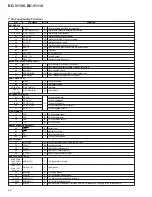
BD-V1100, BD-V1110
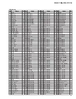
No.
Pin Name
I/O
Function
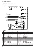
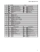
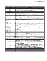
DAC INTERFACE
63
SCLK
O
Bit clock for the DAC
64
LRCLK
Word clock for the DAC
73
PCM_OUT0
Data for the first DAC (left/right)
74
PCM_OUT1
Data for the second DAC (centre/sub)
75
PCM_OUT2
Data for the third DAC (leftsur/rightsur)
IEC958 INTERFACE (S/PDIF)
61
I958OUT
O
S/PDIF signal
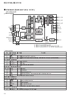
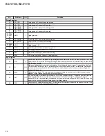
STATUS INFORMATION
PCM RELATED INFORMATION
58
SFREQ
O
When high, indicates that the sampling frequency is either 44.1kHz or 22.05kHz (
∗
).
When low, indicates that the sampling frequency is either 32kHz, 48kHz, 96kHz, 24kHz (
∗
) or 16kHz (*).
(
∗
) : Frequencies available for chips in software versions 4 or later only.)
60
DEEMPH
O
Indicates if de-emphasis is performed
AUDIO VIDEO SYNCHRONIZATION
62
PTS
O
Indicates that a PTS has been detected, active low.
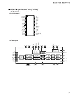
OTHER SIGNALS
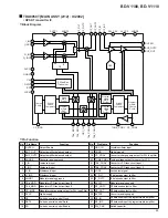
36
CLK
I
Master clock input signal (27MHz)
43
RESET
I(2)
Reset signal input, active low
49
TEST
I(2)
Reserved pin : to be connected to VDD
52
SMODE
I
Reserved pin : to be connected to GND
PIN INTERFACES
26
CLKOUT
O
System clock output
68
VDADAC
VDD Analog DAC PLL supply voltage
69
VCDAC
I
DAC PLL filter
70
VSADAC
GND Analog DAC PLL ground
31
VDASYS
VDD Analog system supply
32
VCSYS
I
System PLL filter
33
VSASYS
GND Analog system ground
5,11,12,24,
27,30,35,
47,50,53,
55,65,71,
76,79
GND
GND Ground
6,10,13,25,
28,29,34,
48,51,54,
56,66,72,
77,78
VDD
VDD Power supply
14
NC
NC
Reserved pin : to be connected GND

