65
BD-V1100, BD-V1110
•
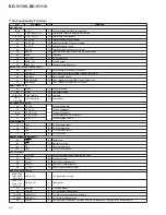
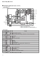
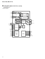
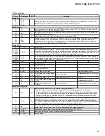
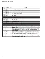
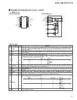
Pin Function
No.
Pin Name
I/O
Function
Analog Video
5
4
10
11
VI_1A
VI_1B
VI_2A
VI_2B
I
Analog video inputs. Up to four composite inputs or two s-video inputs or a combination of the two. The
inputs must be AC coupled. The recommended coupling capacitor is 0.1
µ
F.
Clock Signals
40
PCLK
O
Pixel clock output. The frequency is 12.2727MHz for square-pixel NTSC, 14.75MHz for square-pixel PAL
and 13.5MHz for ITU-R BT.601 sampling modes.
39
PREF
O
Clock phase reference signal. This signal qualifies clock edges when SCLK is used to clock data that is
changing at the pixel clock rate.
38
SCLK
O
System clock output with twice the frequency of the pixel clock (PCLK).
35
36
XTAL1
XTAL2
I
External clock reference, The user may connect XTAL1 to a TTL-compatible oscillator or to one terminal of
a crystal oscillator. The user may connect XTAL2 to the other terminal of the crystal oscillator or not
connect XTAL2 at all. Square pixel sampling uses an oscillator frequency of 26.800MHz. ITU-RBT.601
sampling uses an oscillator frequency of 24.576MHz.
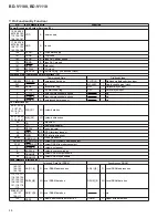
Digital Video
61
EXT_DATA_8
I
Data port-bit [8]
51,52,53,
55,56,58,
59,60
UV[0]-[7]
I/O
8-bit digital chrominance outputs. These terminals may be placed in a high-impedance state under host
port control. These terminals may also be configured to output data from the channel 2 A/D converter. The
function of these terminals is controlled via the gost port-bus. A vendor modifiable subsystem ID may be
configured by configuring the UV[7]-[0] terminals with pull-up/pull-down resistors.
41,42,43,
45,46,48,
49,50
Y[0]-[7]
O
8-bit digital luminance outputs or 8-bit multiplexed luminance and chrominance outputs. These terminals
may be placed in a high-impedance state under host port control. These terminals may also be configured
to output data from the channel 1 A/D converter.
HOST PORT-bus
VMI
I2C
VIP
73
A0
I
VMI address port
74
A1
I
VMI address port
72-69,67,
66,64,63
D[0]-[7]
I/O
VMI data port-bit[7]-[0]
80
INTREQ
0(OD) Interrupt request (INTREQ)
Interrupt request (VIRQ)
79
VC0
I/O
(OD)
VMI port data ack or ready signal
(DTACK)
Serial clock (SCL)
Hardware address bit-0 (HAD[0])
76
VC3
I
VMI port chip select. (VC)
Slave address select (I
2
CA)
VIPCLK
77
VC2
I/O
(OD)
VMI port data strobe or read signal
(DS/RD)
78
VC1
I/O
VMI port read-write or write
(RW/WR)
Serial data (SDA)
Hardware address bit-1 HAD[1]
Hardware control (HCTL)
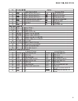
Miscellaneous Signals
26
GPCL
I/O
General purpose control logic. This terminal has three functions :
1. General purpose output. In this mode state of GPCL is derectly programmed via host port.
2. Vertical blank output. In this mode the GPCL terminal is used to indicate the vertical blanking interbal
of the output video. The begining and end times of this signal are programmable via host port control.
3. Sync lock control input. In this mode when GPCL is high the output clocks and horizontal line count
are forced to nominal values.
31
GLCO
I/O
This serial output carries the internal horizontal PLL the color subcarrier PLL phase information and
NTSC/PAL field sequence information. A slave device can decode the information to allow genlocking to
the TVP5010. Data is transmitted at the SCLK rate. Additionally, this terminal in conjunction with PALI and
FID is used to detemine the host port mode configuration during initial power up.
62
OEB
I
Output enable, active low : or data input for 9 or 10-bit external A/D. When this terminal is an output
enable a logic 1 input forces Y and UV output terminals to high impedance states.
28
PLL_BYP
−
Connected to ground side of capacitor between this terminal and PLL_AVDD.
23
RSTINB
I
Reset input, active low. A low input initiates the reset sequence
1,2,13-15 No Connect
−
Not connected

