3
CX-683
2) RF Amplifier
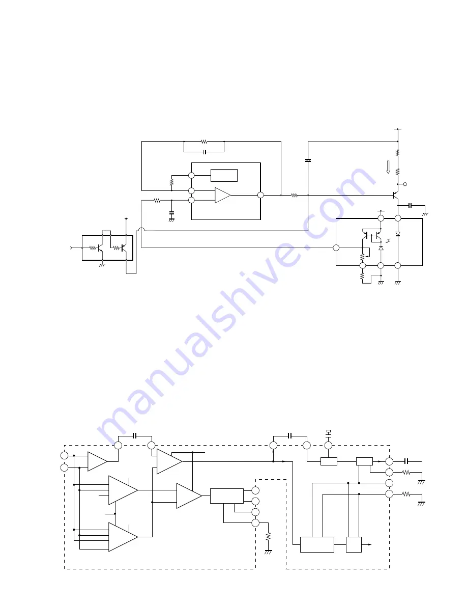
I and J signals being I-J converted in the pickup are entered to 1 and 2 pins. Then, their difference signal (group
signal) and sum signal (bit signal) are generated on RFA1 and RFA2, respectively.
RFA2 and RFA3 are switching operational amplifiers. The amplifiers detect high reflection (Premastered) and low
reflection (Recordable) using the disc detector switch (S404) to switch to the gain selected by the serial command
HLPT or PTGR.
RF signal (46 pin) is operated and conducted to the AGC circuit and equalizer via C122 to generate RF signal (36 pin).
RF signal is maintained essentially at a constant level (approximately at 1.1 Vpp) by the AGC circuit.
This signal is entered to the signal processing LSI (IC201: 55 pins) for the data processing as well as control of the
Premastered Disc playing spindle.
1) APC (Automatic Power Control) Circuit
Since laser diode (LD) has temperature characteristics, the APC circuit is provided to control current flow using the
monitor diode so that the output may be kept at a constant level.
LD current is determined by measuring voltage across V1 and 3VD.
The current value should be approximately 40 mA (0.4V/10
Ω
).
19
20
6
10
12
11
–
+
21
12
14
13
VREF
Q102
UMD2N
LDCNT
R103
PD
APC REF
CXA2523AR
MON
Vr
MD
LD
3VD
C105
R1
LD+
3VD
R102 0R0
R101 10
VI
100/6R3
R108
APC
C108 R001
R109 470K
R110
6R8K
1.25V
6R8K
C106
+
GND
VR
R104
0
Ω
LD –
PU unit
47K
C107
3VP
22P
1
2
38
–
+
–2
–1
–1
–2
–1
–2
–1
–1
–1
–2
–2
48
47
22
20
22
46
40
39
25
20
36
37
Peak/Bottom
Hold
BPF
fo=720kHz
Peak
Hold
BPF3T
PEAK3T
PBH1
J
MORFO
MORFI
RFO
I
RFA1
OFST
ABCD
RFA3
PEAK
BOTM
F0CNT
WBLADJ
PBSW
GRVA
HLPT
GRV
RFA2
PTGR
AGC
EQA
3TADJ
F0CNT
I3
EQADJ
RFAGC
<To IC201>
RF
C122
R022
C124
R047


