Summary of Contents for DEQ-P6600/EW

Page 1: ...RATION 2004 DEQ P8000 UC CRT3263 MULTI CHANNEL AV PROCESSOR DEQ P8000 UC DEQ P6600 EW DEQ P7650 ES Manufactured under license from Dolby Laboratories Dolby Pro Logic and the double D symbol are trademarks of Dolby Laboratories DTS and DTS Digital Surround are registered trademarks of Digital Theater Systems Inc This product cannot be operated independently Combining DVH P5000MP UC etc for performi...

Page 2: ...leaning should be made securely When you find the procedures bearing any of the symbols be sure to fulfill them 2 Adjustments To keep the original performances of the product optimum adjustments or specification confirmation is indispensable In accordance with the procedures or instructions described in this manual adjustments should be performed 3 Cleaning For optical pickups tape deck heads lens...

Page 3: ...AGRAM AND SCHEMATIC DIAGRAM 12 3 1 BLOCK DIAGRAM 12 3 2 OVERALL CONNECTION DIAGRAM GUIDE PAGE 14 4 PCB CONNECTION DIAGRAM 20 4 1 AUDIO CONTROL UNIT 20 5 ELECTRICAL PARTS LIST 24 6 ADJUSTMENT 31 7 GENERAL INFORMATION 32 7 1 DIAGNOSIS 32 7 1 1 DISASSEMBLY 32 7 1 2 CONNECTOR FUNCTION DESCRIPTION 33 7 2 IC 34 7 3 OPERATIONAL FLOW CHART 41 7 4 CLEANING 42 8 OPERATIONS 43 ...

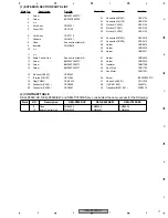
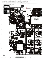
Page 4: ...DEQ P8000 UC 4 1 2 3 4 1 2 3 4 C D F A B E 1 SPECIFICATIONS ...

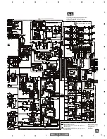
Page 5: ...DEQ P8000 UC 5 5 6 7 8 5 6 7 8 C D F A B E ...

Page 6: ...DEQ P8000 UC 6 1 2 3 4 1 2 3 4 C D F A B E ...

Page 7: ...DEQ P8000 UC 7 5 6 7 8 5 6 7 8 C D F A B E ...

Page 8: ...ked by are generally unavailable because they are not in our Master Spare Parts List Screw adjacent to mark on the product are used for disassembly For the applying amount of lobricants or glue follow the instructions in this manual In the case of no amount instructions apply as you think it appropriate ...

Page 9: ...Card See contrast table 2 21 4 Card See contrast table 2 21 5 Owner s Manual See contrast table 2 21 6 Warranty Card See contrast table 2 22 Cable CDE6366 23 Clamper CNV1272 24 Clamper CNV1343 Mark No Description Part No Mark NO Description DEQ P8000 UC DEQ P6600 EW DEQ P7650 ES 10 Polyethylene Bag CEG1160 Not used CEG1160 11 Polyethylene Bag CEG1173 CEG 162 CEG 162 13 Carton CHG5244 CHG5243 CHG52...

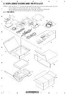
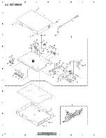
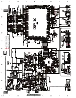
Page 10: ...DEQ P8000 UC 10 1 2 3 4 1 2 3 4 C D F A B E 2 2 EXTERIOR ...

Page 11: ...CKB1053 17 Terminal CN103 CKF1064 18 Plug CN801 CKM1432 19 Connector CN101 CKS2600 20 Connector CN102 CKS2601 21 Connector CN961 CKS3124 22 Connector CN172 CKS3125 23 Pin Jack CN122 CKS3144 24 Pin Jack CN751 CKS3144 25 Pin Jack CN752 CKS3144 26 Connector CN201 CKS3410 27 Connector CN202 CKS3413 28 Holder CNC9810 29 Holder CND2230 30 Holder CND2231 31 Holder CND2232 32 Holder CND2233 33 Insulator C...

Page 12: ...50 SYS PW DSP MUTE AMP MUTE NAVIMUTE SOURCE 10 12 47 VST2 VST VDT VCK DAML DACLK DATX DARST 53 54 55 GSST GSDT GSCK 15 8 IP BUS DRIVER TX RX IC602 S 80835CNUA B8U RESET DVDD 2 1 DVDD S601 RESET RSTMUTE Q601 2SA1576 5V 3V OR 3V 5V IC551 TC74VHC08FT IC552 TC74VHC541FT IC553 TC74VHCT541AFT DRAM IC252 MSM51V4265EP 70TS IC221 AK7730VT XTI LRCLKI BITCLK SDDATA 15 14 36 4 5 13 14 LRCLK BCK 26 X251 24 576...

Page 13: ...705 AMP RR RL 3 5 1 7 AMP SW C FR FL RR RL LFE CENTER 3 5 1 7 AMP 1 7 30 32 EVOL L CH AND CENTER IC501 PML011A CDL CDR NAVI SPKR1L SPKR1R SPKR2R EVOL R CH AND LFE IC502 PML011A CDL CDR NAVI SPKR1L SPKR1R SPKR2R 4 25 25 4 22 22 IC801 IC802 PAL007A AMP FR FR FL FL FLIN FRIN STBY MUTE AMP RL RL RR RR C C RRIN RLIN CIN STBY MUTE B REM IC802 IC801 SYSPW A 8V ERRMUTE DSPMUTE Q505 IMD2A Q504 DTA124EU A 8...

Page 14: ...C TESTTX TESTRX testin TESTCLK AKTX AKRX AKCLK AEQTEST NC NC NC NC NC NC SELSW MICSENS ROMCS ROMDATA ROMCLK NC NC NC NC SOURCE NC NAVIMUTE MUTERQ gainstb dacrst dacml DSPMUTE GAINTX GAINCK DACCLK DACTX SYSPW DSPPW ysslock DACRX AKDRDY AKRDY 32KSW AKCKS1 aksrst akirst akrq yssr1 yssic ysscs CKSO NC YSSRX YSSTX NAVISENS NC NC evolstb2 evolstb1 reset nmi bsens asens SYSTEM CONTROLLER RESET O O O O O ...

Page 15: ...e to use parts of identical designation Symbol indicates a resistor No differentiation is made between chip resistors and discrete resistors NOTE Symbol indicates a capacitor No differentiation is made between chip capacitors and discrete capacitors A AUDIO CONTROL UNIT FAN 600µH DAC E VOL E VOL MUTE POWER AMP HI OUT PRE OUT The power supply is shown with the marked box ANALOG 34 0dBs O A O A O A ...

Page 16: ...DEQ P8000 UC 16 1 2 3 4 1 2 3 4 C D F A B E A a A b A a A a A b 1 2 O O O O O O O O O O O O O O O O O O A A A A A A A A A A A A A A A O A OPTICAL SIGNAL LINE ANALOG SIGNAL LINE ANALOG 8dBs ...

Page 17: ...EQTEST NC NC NC NC NC NC SELSW MICSENS ROMCS ROMDATA ROMCLK NC NC NC NC SOURCE NC NAVIMUTE MUTERQ gainstb dacrst dacml DSPMUTE GAINTX GAINCK DACCLK DACTX SYSPW DSPPW ysslock DACRX AKDRDY AKRDY 32KSW AKCKS1 aksrst akirst akrq yssr1 yssic ysscs CKSO NC YSSRX YSSTX NAVISENS NC NC evolstb2 evolstb1 reset nmi bsens asens SYSTEM CONTROLLER RESET A A A ...

Page 18: ...component parts indicates the importance of the safety factor of the part Therefore when replacing be sure to use parts of identical designation A AUDIO CONTROL UNIT 600µH MUTE POWER AMP PRE OUT The power supply is shown with the marked box ANALOG 34 0dBs O A O A O A O O O O O A A A ANALOG 5 0dBs ...

Page 19: ...xpressed as 2 2 2R2 0 022 R022 Symbol indicates a resistor No differentiation is made between chip resistors and discrete resistors NOTE Symbol indicates a capacitor No differentiation is made between chip capacitors and discrete capacitors FAN 600µH DAC E VOL E VOL HI OUT O A O A O A ANALOG 16 2dBs ANALOG 8 0dBs ANALOG 5 0dBs ANALOG 2 3dBs ...

Page 20: ...p Part A A AUDIO CONTROL UNIT SIDE B SIDE A NOTE FOR PCB DIAGRAMS 1 The parts mounted on this PCB include all necessary parts for several destination For further information for respective destinations be sure to check with the schematic dia gram 2 Viewpoint of PCB diagrams FRO OPT1 IN RCA IN MIC IN IP BUS OUT IP BUS IN RESET ...

Page 21: ...DEQ P8000 UC 21 5 6 7 8 5 6 7 8 C D F A B E A SIDE A IC Q FRONT PREOUT REAR PREOUT CENTER LFE CORD ASSY OPT2 IN FAN ...

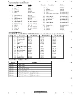
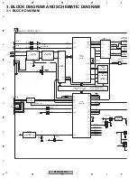
Page 22: ...DEQ P8000 UC 22 1 2 3 4 1 2 3 4 C D F A B E A A AUDIO CONTROL UNIT IC Q ...

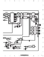
Page 23: ...DEQ P8000 UC 23 5 6 7 8 5 6 7 8 C D F A B E A SIDE B ...

Page 24: ... IC S 812C56AUA C3K IC 941 IC PQ1X331M2ZP IC 981 IC PQ1X251M2ZP IC 982 IC BA033FP Q 101 Transistor 2SC2412K Q 102 Transistor 2SC2412K Q 121 Transistor DTC124EU Q 174 Transistor 2SC2412K Q 501 Transistor FMG12 Q 502 Transistor FMG12 Q 503 Transistor FMG12 Q 504 Transistor DTA124EU Q 505 Transistor IMD2A Q 601 Transistor 2SA1576 Q 681 Transistor 2SC2412K Q 682 Transistor 2SC2412K Q 751 Transistor 2S...

Page 25: ...2 Inductor CTF1473 L 553 Inductor CTF1473 L 601 Inductor CTF1473 L 602 Inductor CTF1473 L 751 Inductor CTF1487 L 752 Inductor CTF1473 L 753 Inductor CTF1473 L 754 Inductor CTF1473 L 755 Inductor CTF1473 Circuit Symbol and No Part No L 756 Inductor CTF1473 L 757 Inductor CTF1473 L 801 Choke Coil 600µH CTH1275 L 901 Coil CTH1267 L 902 Coil CTH1267 L 903 Coil CTH1267 X 251 Radiator 24 576MHz CSS1630 ...

Page 26: ...R 363 RS1 16S1002D R 364 RS1 16S1002D R 365 RS1 16S3901D Circuit Symbol and No Part No R 366 RS1 16S3901D R 367 RS1 16S822J R 368 RS1 16S822J R 369 RS1 16S1502D R 370 RS1 16S1502D R 381 RS1 16S8200D R 382 RS1 16S8200D R 383 RS1 16S1002D R 384 RS1 16S1002D R 385 RS1 16S3901D R 386 RS1 16S3901D R 387 RS1 16S822J R 388 RS1 16S822J R 389 RS1 16S1502D R 390 RS1 16S1502D R 401 RS1 16S8200D R 402 RS1 16S...

Page 27: ...3J R 627 RAB4C471J R 628 RS1 16S473J R 629 RS1 16S473J R 630 RAB4C471J R 631 RS1 16S474J Circuit Symbol and No Part No R 632 RAB4C101J R 633 RAB4C471J R 634 RS1 16S473J R 635 RS1 16S473J R 636 RS1 16S471J R 637 RS1 16S473J R 638 RAB4C471J R 639 RS1 16S471J R 640 RS1 16S473J R 641 RS1 16S102J R 642 RS1 16S104J R 643 RAB4C101J R 644 RS1 16S0R0J R 645 RS1 16S0R0J R 646 RS1 16S102J R 647 RAB4C102J R 6...

Page 28: ...6S102J R 961 RS1 16S101J R 962 RS1 16S101J R 981 RS1 16S473J R 982 RS1 16S332J R 983 RS1 16S472J Circuit Symbol and No Part No CAPACITORS C 101 CKSRYB104K25 C 102 CKSRYB104K25 C 103 CKSRYB104K25 C 104 CCSRCH470J50 C 105 CCSRCH470J50 C 106 CKSYB106K6R3 C 107 CKSYB106K6R3 C 121 CKSYB106K6R3 C 122 CCSRCH470J50 C 123 CCSRCH470J50 C 124 CKSYB106K6R3 C 125 CCSRCH150J50 C 126 CKSYB106K6R3 C 127 CEVW100M1...

Page 29: ...4 CKSRYB102K50 C 385 CCSRCH121J50 C 386 CCSRCH121J50 C 387 CKSRYB105K10 C 388 CKSRYB105K10 Circuit Symbol and No Part No C 401 CKSRYB472K50 C 402 CKSRYB104K25 C 403 CKSRYB102K50 C 404 CKSRYB473K50 C 405 CCSRCH470J50 C 406 CCSRCH150J50 C 407 CCSRCH121J50 C 408 CKSRYB472K50 C 409 CEVWNP100M10 C 410 CEVWNP100M10 C 411 CKSRYB105K10 C 412 CKSRYB105K10 C 413 CKSRYB105K10 C 414 CKSRYB105K10 C 451 CCSRCH4...

Page 30: ...817 CKSRYB105K10 C 818 CKSRYB105K10 C 819 CKSRYB105K10 C 820 4700µF 16V CCH1068 P35 C 823 CKSRYB105K10 C 824 CKSRYB105K10 C 825 CKSQYB225K10 C 826 CKSYB475K16 C 901 CCSRCH151J50 C 902 CKSRYB104K25 C 903 CKSRYB104K25 C 904 CKSRYB104K25 C 905 CCSRCH101J50 C 906 CCSRCH471J50 C 907 CKSRYB104K25 Circuit Symbol and No Part No C 908 CEHVW330M16 C 909 CEHVW330M16 C 910 CKSYB475K10 C 911 CKSYB225K16 C 912 ...

Page 31: ...DEQ P8000 UC 31 5 6 7 8 5 6 7 8 C D F A B E 6 ADJUSTMENT There is no information to be shown in this chapter ...

Page 32: ...oving the Case Fig 1 Case Fig 2 Audio Control Unit Removing the Audio Control Unit Fig 2 Remove the screw 1 Remove the four screws and then remove the Case 3 4 3 3 Remove the two screws 2 Straighten the tabs at four locations indicated 3 Remove the screw and then remove the Audio Control Unit 4 1 1 1 1 1 2 2 3 ...

Page 33: ...2 GND 3 GND 4 NC 5 BUS 6 GND 7 BUSL 8 ASENB 9 BUSR 10 BUSR 11 BUSL 1 BUS 2 GND 3 GND 4 NC 5 BUS 6 GND 7 BUSL 8 ASENB 9 BUSR 10 BUSR 11 BUSL MAIN INPUT 4 3 2 1 OPTICAL INPUT 1 1 OPT5V 2 GND 3 OPTIN 4 GND 1 2 3 4 OPTICAL INPUT 2 POWER SUPPLY 1 OPT5V 2 GND 3 OPTIN 4 GND 1 RL 2 FL 3 RL 4 FL 5 RR 6 FR 7 RR 8 FR 9 CENTER 10 NC 11 CENTER 12 B REMOTE 13 GND 14 GND 15 B UP 16 GND AUTO EQ 1 3 5 7 9 11 13 2 ...

Page 34: ...VSS 2 Q0 3 I M Counter 11bit Pll XN 1 _ 2 Fuse Select 8 7 6 IN VREF VCC 3 4 5 S C P GND OUT 10 9 FB IN 1 2 CT RT Error amp S C P comp 2 46V 0 5V VREF 1 83V 11 1V Reference supply Triangular wave OSC Clamp S R Latch R O U V L O PWM comparator I OE A1 B1 GND 1 2 3 4 8 7 6 5 VCC C1 D1 EX IC s marked by are MOS type Be careful in handling them because they are very liable to be damaged by electrostati...

Page 35: ...n for digital section 3 3V typ 22 DVSS Ground pin for digital section 0V 23 24 CLKO1 2 O Clock output pin 25 XTO O Crystal oscillator output pin 26 XTI I Master clock input pin 27 DVSS Ground pin for digital section 0V 28 DVDD Power supply pin for digital section 3 3V typ 29 SMODE I Slave Master mode selector pin 30 SO O Serial data output pin for Microcomputer interfaces 31 SI I Microcomputer int...

Page 36: ...RAMA17 OVFB END RAMA15 RAMA16 RAMA13 RAMA14 VDD2 RAMA12 DDIN3 TESTXI TESTBRK AVSS TESTR2 TESTR1 VDD2 XO DDIN0 XI DDIN2 DDIN1 SDBCKI0 DIRPRO VSS SDWCKI0 AVDD CPO VDD1 DIRPCO IPORT1 IPORT0 IPORT3 IPORT2 TESTXO IPORT4 TESTXEN TESTMS VSS VDD2 VDD1 AC3DATA KARAOKE SDOA2 SDIA SDOA0 SDOA1 SDIB2 SDIB3 SDIB0 SDIB1 101 102 99 100 97 98 95 96 93 94 91 92 89 90 87 88 85 86 83 84 81 82 79 80 77 78 75 76 73 74 ...

Page 37: ...C A S N R A S N R A M W E N R A M O E N R A M A 0 1 7 O V F B E N D SDOB3 SDOB2 SDOB1 SDOB0 SDWCKI1 SDBCKI1 OPORT0 7 CS S O SI S C K IPORT0 4 D B L ERR BS SYNC U FS128 C SYNC U FS128 C VMOD BSMOD DDINSEL UMOD IPORT5 7 7 6 5 CMOD CRC PLL PLL DIR SDIASEL MainDSP AC 3 ProLogicII DTS Decoder Coefficient Program RAM SDIBSEL SubDSP SDIBCKSEL SDOBCKSEL OVFSEL Control Resistor MPLOAD Microcomputer Interfa...

Page 38: ... OUT 3 ML MC MDI MDO NC NC V CC 0 AGND0 V CC 1 AGND1 V CC 2 AGND2 1 2 3 4 5 6 7 8 9 10 11 12 36 35 34 33 32 31 30 29 28 27 26 25 LRCK BCK DATA1 VOUT1 2 DATA2 VOUT3 4 DATA3 VOUT5 6 ML MC MDI MDO RST SCKI SCKO VOUT1 VOUT2 VOUT3 VOUT4 VOUT5 VOUT6 ZEROA ZERO1 GPO1 ZERO6 GPO6 2ch LFP Output Amp DAC CAP1 CAP2 Malti Level Module DAC DAC 2ch LFP Output Amp 2ch LFP Output Amp 3 3V Power supply 5V BPZ Contr...

Page 39: ...s Driver power supply switch output IPBus Data input IPBus Communication data output AEQ test mode Data output AEQ test mode Factory test mode Data input Factory test mode CLK input Factory test mode Judgment AK7730 Communication data output AK7730 Communication data input AK7730 Communication CLK H AEQ test mode L Normal mode Not used Jack sense for NAVI guide mixing L Jack Not used Analog input ...

Page 40: ...r clock selection pin 1 AK7730 System reset pin AK7730 Initial reset pin AK7730 Request pin YSS PLL initialization signal output terminal YSS Reset terminal YSS Chip select AK7730 Clock switch Analog GND Not used A D Reference voltage Analog power supply YSS Communication data input YSS Communication data output YSS PLL lock detection terminal DAC Communication data input DACRX AKRDY PD5967A 60 61...

Page 41: ...6 7 8 5 6 7 8 C D F A B E 7 3 OPERATIONAL FLOW CHART VCC 5V Pin 13 78 Power ON bsens L asens L bsens Pin 15 Completes power on operation SYSPW H Pin 60 DSPPW H Pin 61 Source ON asens Pin 16 MUTERQ H Pin 51 IPPW H Pin 21 ...

Page 42: ...1 2 3 4 1 2 3 4 C D F A B E 7 4 CLEANING Before shipping out the product be sure to clean the following portions by using the prescribed cleaning tools Portions to be cleaned Fans Cleaning tools Cleaning paper GED 008 ...

Page 43: ... with power regardless of ignition switch position Fuse holder Black ground To vehicle metal body Blue white To system control terminal of the power amp or Auto antenna relay control terminal max 300 mA 12 V DC Do not connect anything to the speaker leads that are not connected to speakers When you connect a power amp sold separately be sure to use the blue white lead of this unit If you use the b...

Page 44: ...speaker Center speaker Subwoofer System remote control RCA cables sold separately Power amp sold separately Subwoofer output Rear output Front output Center output Power amp sold separately Power amp sold separately Power amp sold separately When you connect a power amp sold separately be sure to use the blue white lead of this unit If you use the blue white lead of the head unit it causes noises ...

Page 45: ... g CD TS37GP sold separatly IP BUS cable supplied A V BUS cable supplied with TV tuner IP BUS cable supplied with multi DVD player RCA cable supplied with multi DVD player Optical cable sold separately Hide away TV tuner e g GEX P6400TV sold separately Multi DVD player e g XDV P90 sold separately AV Receiver DVD player AVH P6600DVD Hide away unit sold separately 26 pin cable Blue Navigation unit e...

Page 46: ...DEQ P8000 UC 46 1 2 3 4 1 2 3 4 C D F A B E Jigs List Cleaning paper GED 008 Cleaning fans Name Jig No Remarks g ...

Reviews: