background image

32

DEQ-P9

DSP Unit

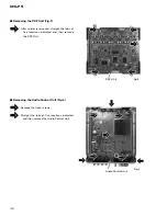
Fig.3

-

Removing the DSP Unit (Fig.3)

After solder is removed, straight the tabs at

five locations indicated and then remove

the DSP Unit.

Fig.4

-

Removing the Audio Control Unit (Fig.4)

Remove the three screws.

Straight the tabs at five locations indicated

and then remove the Audio Control Unit.

Audio Control Unit

Summary of Contents for DEQ-P9

Page 1: ...NEER CORPORATION 2001 K ZZA MAY 2001 Printed in Japan ORDER NO CRT2686 UNIVERSAL DIGITAL PREAMP EQUALIZER DEQ P9 UC EW Service Manual CONTENTS 1 SAFETY INFORMATION 2 2 EXPLODED VIEWS AND PARTS LIST 2 3 BLOCK DIAGRAM AND SCHEMATIC DIAGRAM 6 4 PCB CONNECTION DIAGRAM 16 5 ELECTRICAL PARTS LIST 24 6 ADJUSTMENT 30 7 GENERAL INFORMATION 31 7 1 DIAGNOSIS 31 7 1 1 DISASSEMBLY 31 7 1 2 CONNECTOR FUNCTION D...

Page 2: ...reliability of the product and may void the warranty If you are not qualified to perform the repair of this product properly and safely you should not risk trying to do so and refer the repair to a qualified service technician WARNING This product contains lead in solder and certain electrical parts contain chemicals which are known to the state of California to cause cancer birth defects or other...

Page 3: ...lamper CNV1272 26 Filter See Contrast table 2 Mark No Description Part No Mark No Description Part No 1 PACKING SECTION PARTS LIST NOTE Parts marked by are generally unavailable because they are not in our Master Spare Parts List Screws adjacent to mark on the product are used for disassembly 2 CONTRAST TABLE DEQ P9 UC and EW are constructed the same except for the following Part No Mark No Symbol...

Page 4: ...4 DEQ P9 2 2 EXTERIOR A B ...

Page 5: ...8 20 Terminal CN902 CKE1033 21 Fuse Holder CN901 CKR1021 22 Connector CN602 CKS2248 23 Connector CN601 CKS2601 24 Connector CN604 CKS3410 25 Shield CNC4761 26 Holder CNC9161 27 Holder CNC9162 28 Holder CNC9163 29 Screw PPZ20P060FZK 30 Screw PPZ30P080FZK 31 DSP Unit UC CWX2519 DSP Unit EW CWX2520 32 Connector CN1700 CKS1956 33 Connector CN1000 CKS2191 34 Connector CN1701 CKS2198 35 Connector CN1702...

Page 6: ...3 2 1 2 1 2 Q50 Q52 Q51 Q66 Q86 Q68 Q67 Q88 Q87 Q604 EF902 EF903 EF904 EF906 EF905 T86 IC 66 TL1451ANS M IC 50 TL5001CPS Q53 Q54 B VDD VDD OUT IN 9 10 2 4 1 7 T66 Q901 5 A 8V A 5V A 5V D 5V D 5V A 8V 2 4 8 7 6 5 2 4 8 7 6 23 24 34 26 27 28 48 DIRRST 3 DIN0 13 65 68 69 72 14 15 1 3 6 1 3 6 1 3 6 1 3 6 3 CKOUT BCK LRCK 16 70 71 DATAO FS2 FS1 FS0 DIRERR DIRPCM DEEH D 5V VDD BU X1000 12 288MHz IC 1003...

Page 7: ...EMPL DEMPR 20 DEEM2 DOL1 DOL2 IC 1411 PCM1704U J IC 1410 PCM1704U J IC 1511 PCM1704U J IC 1510 PCM1704U J 19 DEEM1 3 DOL 43 MUTER 42 MUTEL 2 1 1 1 1 DOR 37 DEMPL 36 DEHPR 32 33 DOR1 DOR2 30 31 HIGH RCH HIGH LCH 7 1 LOW RCH LOW LCH 1 3 1 1 HL HR MR ML LL LR SR SL 4 5 8 3 4 6 4 6 7 9 7 9 10 12 10 12 13 16 25 SW RCH SW LCH IC 1300 SM5847AF IC 1400 PD7010A1 IC 1500 SM5847AF IC 1600 PCM1716E 3 CN1702 C...

Page 8: ...ure to refer to EXPLODED VIEWS AND PARTS LIST or ELECTRICAL PARTS LIST A 22µH 22µH 22µH DAN202U D607 MODE CN1700 C SYSTEM CONTROLLER DC DC CONVERTER 4 9V 8 5 8 1V FM 100 EW 0 1dBs FM 100 UC 4 1dBs AM 30 EW 10 1dBs AM 30 UC 14 1dBs IP BUS 1 9dBs OPTICAL 5 9dBs IP BUS MCD MDVD OPTICAL SCD OPT MCD OPT DVD ...

Page 9: ... chip capacitors and discrete capacitors E VOL E VOL PRE AMPLIFIER x4 8 1V 5 1V 8 1V 5 1V 14 4V AUDIO CONTROL UNIT RCA OUTPUT RCA OUTPUT The mark found on some component parts indicates the importance of the safety factor of the part Therefore when replacing be sure to use parts of identical designation B REM A B FM EW 2 42dBs FM UC 0 42dBs AM EW 5 58dBs AM UC 9 58dBs IP BUS 6 42dBs OPTICAL 6 42dB...

Page 10: ...10 DEQ P9 1 2 3 4 1 2 3 4 D C B A 3 3 DSP UNIT GUIDE PAGE CN602 CN603 DIR OPTICAL IN A a A b A a A a A b A b A b A b A a A a Large size SCH diagram Guide page Detailed page B B a ...

Page 11: ...IT A AUDIO CONTROL UNIT DF DAC I V CONVERTER DIGITAL ANALOG 8 1V 8 1V 4 9V 5 1V 0V FM EW 0 58dBs FM UC 4 58dBs AM EW 10 58dBs AM UC 14 58dBs IP BUS 1 42dBs OPTICAL 5 42dBs FM EW 0 1dBs FM UC 4 1dBs AM EW 10 1dBs AM UC 14 1dBs IP BUS 1 9dBs OPTICAL 5 9dBs B b B ...

Page 12: ...12 DEQ P9 1 2 3 4 1 2 3 4 D C B A CN603 OPTICAL IN B a B b B a 1 ...

Page 13: ...13 DEQ P9 5 6 7 8 5 6 7 8 D C B A CN602 DIR B a B b B a 2 ...

Page 14: ...14 DEQ P9 1 2 3 4 1 2 3 4 D C B A CN501 x 6 B DSP UNIT DAC DIGITAL ANALOG FM EW 0 58dBs FM UC 4 58dBs AM EW 10 58dBs AM UC 14 58dBs IP BUS 1 42dBs OPTICAL 5 42dBs B a B b B b 1 ...

Page 15: ...Q P9 5 6 7 8 5 6 7 8 D C B A CN903 A AUDIO CONTROL UNIT DF I V CONVERTER DIGITAL ANALOG 8 1V 8 1V 4 9V 5 1V 0V FM EW 0 1dBs FM UC 4 1dBs AM EW 10 1dBs AM UC 14 1dBs IP BUS 1 9dBs OPTICAL 5 9dBs B a B b B b 2 ...

Page 16: ...nclude all necessary parts for several destination For further information for respective destinations be sure to check with the schematic dia gram 2 Viewpoint of PCB diagrams Capacitor Connector P C Board Chip Part SIDE A SIDE B 4 PCB CONNECTION DIAGRAM 4 1 AUDIO CONTROL UNIT Fuse RCA OUTPUT RCA OUTPUT Cord Assy ...

Page 17: ...17 DEQ P9 5 6 7 8 5 6 7 8 D C B A A SIDE A IC Q CN1701 B CN1000 B CN1702 B CN1700 B IP BUS INPUT OPTICAL INPUT RESET MODE ...

Page 18: ...18 DEQ P9 1 2 3 4 1 2 3 4 D C B A A AUDIO CONTROL UNIT A ...

Page 19: ...19 DEQ P9 5 6 7 8 5 6 7 8 D C B A A SIDE B ...

Page 20: ...20 DEQ P9 1 2 3 4 1 2 3 4 D C B A 4 2 DSP UNIT B DSP UNIT B CN501 A ...

Page 21: ...21 DEQ P9 5 6 7 8 5 6 7 8 D C B A SIDE A IC Q B CN903 A CN603 A CN602 A ...

Page 22: ...22 DEQ P9 1 2 3 4 1 2 3 4 D C B A IC Q B DSP UNIT B ...

Page 23: ...23 DEQ P9 5 6 7 8 5 6 7 8 D C B A SIDE B B ...

Page 24: ...Q 608 Transistor 2SC2412K Q 609 Transistor IMD2A Q 610 Transistor DTA124EU Q 611 Transistor 2SC2412K Q 901 Transistor 2SB1243 Q 902 Transistor 2SD1760F5 Q 903 Transistor 2SC2412K Q 904 Transistor DTC114EK Q 905 Transistor 2SB1238 D 50 Diode D2FS6 D 66 Diode SC802 06 D 86 Diode SC802 06 D 101 Diode DAP202U D 102 Diode DAP202U D 201 Diode DAP202U D 202 Diode DAP202U D 301 Diode DAP202U D 302 Diode D...

Page 25: ...E2201D R 206 RN1 10SE2201D R 207 RN1 10SE4700D R 208 RN1 10SE4700D R 209 RS1 16S103J R 210 RS1 16S103J R 211 RN1 10SE4700D R 212 RN1 10SE4700D R 213 RS1 16S103J R 214 RS1 16S103J R 215 RN1 10SE2202D R 216 RN1 10SE2202D R 301 RN1 10SE1002D R 302 RN1 10SE1002D R 303 RN1 10SE1201D R 304 RN1 10SE1201D R 305 RN1 10SE2201D R 306 RN1 10SE2201D R 307 RS1 16S103J R 308 RS1 16S103J R 309 RN1 10SE4700D R 310...

Page 26: ...H1396 C 104 10µF 16V CCH1396 C 105 CCSRCH471J50 C 106 CCSRCH471J50 C 107 10µF 16V CCH1396 C 109 10µF 16V CCH1396 C 111 CKSRYB104K25 C 112 CKSRYB104K25 C 201 CFHSQ221J50 C 202 CFHSQ221J50 C 203 10µF 16V CCH1396 C 204 10µF 16V CCH1396 C 205 CCSRCH471J50 C 206 CCSRCH471J50 C 207 10µF 16V CCH1396 C 208 10µF 16V CCH1396 C 211 CKSRYB104K25 C 212 CKSRYB104K25 C 301 CFHSQ221J50 C 302 CFHSQ221J50 C 303 10µ...

Page 27: ... D 1412 Diode Network DA204U D 1413 Diode Network DA204U D 1500 Diode Network DA204U D 1501 Diode Network DA204U D 1510 Diode Network DA204U D 1511 Diode Network DA204U D 1512 Diode Network DA204U D 1513 Diode Network DA204U D 1600 Diode Network DA204U D 1601 Diode Network DA204U D 1700 Diode MA111 L 1000 Inductor CTF1295 L 1002 Inductor LCTA1R0J4532 L 1003 Inductor LCTA1R0J4532 L 1004 Inductor CT...

Page 28: ...S0R0J R 1114 RAB4C471J R 1115 RAB4C471J R 1116 RAB4C471J R 1117 RAB4C471J R 1118 RAB4C473J R 1119 RAB4C473J R 1120 RS1 16S105J R 1121 RS1 16S105J R 1122 RS1 16S331J R 1123 RS1 16S331J R 1124 RS1 16S0R0J R 1125 RS1 16S0R0J R 1126 RS1 16S0R0J R 1127 RS1 16S0R0J R 1128 RS1 16S0R0J R 1129 RS1 16S0R0J R 1130 RAB4C473J R 1133 RAB4C473J R 1134 RS1 16S0R0J R 1135 RS1 16S0R0J R 1136 RS1 16S0R0J R 1137 RS1 ...

Page 29: ...6 C 1129 CEJQ470M6R3 C 1130 CCSRCH100D50 C 1132 CKSRYB473K25 C 1134 CKSRYB473K25 C 1136 CKSRYB102K50 C 1138 CKSRYB473K25 C 1140 CKSRYB473K25 C 1141 CKSRYB102K50 C 1142 CKSRYB473K25 C 1143 CKSRYB473K25 C 1144 CKSRYB473K25 C 1146 CKSRYB473K25 C 1300 CKSRYB104K25 C 1301 CKSRYB104K25 C 1302 CKSRYB104K25 C 1303 CCSRCH331J50 C 1304 CKSRYB104K25 C 1305 CKSRYB104K25 C 1306 CEZA330M16 C 1307 CKSRYB473K25 C...

Page 30: ...5 C 1518 CEZA220M25 C 1519 CEZA220M25 C 1520 CEZA101M10 C 1521 CEZA101M10 C 1522 CKSRYB104K25 C 1523 CKSRYB104K25 C 1524 CEZA470M10 C 1525 CEZA470M10 C 1526 CKSRYB104K25 C 1527 CKSRYB104K25 C 1528 CEZA470M10 C 1529 CEZA470M10 C 1530 CEZA470M10 C 1531 CEZA470M10 C 1532 CKSRYB104K25 C 1533 CKSRYB104K25 C 1534 10µF 16V CCH1352 C 1535 10µF 16V CCH1352 C 1536 CFHSQ331J50 C 1537 CFHSQ331J50 C 1538 CFHSQ...

Page 31: ...AGNOSIS 7 1 1 DISASSEMBLY Case Fig 1 Removing the Case Fig 1 Remove the eleven screws and then remove the Case Fig 2 Removing the DSP Section Fig 2 Remove the four screws Disconnect the connector and then remove the DSP Section DSP Section ...

Page 32: ...lder is removed straight the tabs at five locations indicated and then remove the DSP Unit Fig 4 Removing the Audio Control Unit Fig 4 Remove the three screws Straight the tabs at five locations indicated and then remove the Audio Control Unit Audio Control Unit ...

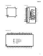
Page 33: ...OUT1 OUT2 OUT3 OUT4 OUT5 OUT6 DATA CLK STB PM0017AM 7 1 2 CONNECTOR FUNCTION DESCRIPTION IP BUS INPUT 11 10 9 8 7 6 5 4 3 2 1 1 BUS 2 GND 3 GND 4 NC 5 BUS 6 GND 7 BUS L INPUT 8 ASENB 9 BUS R INPUT 10 BUS R INPUT 11 BUS L INPUT 4 3 2 1 1 GND 2 GND 3 NC 4 OPTOUT OPTICAL INPUT IC s marked by are MOS type Be careful in handling them because they are very liable to be damaged by electrostatic induction...

Page 34: ... IF DC 4 15V 1 65V AC 2Vrms 0 8Vrms b Linedriver amplifier differential mono input circuit Quasi differential stereo input circuit Mix Bypass Selector Bypass gain b Volume 6ch independent control Zero cross d etect 6ch independent control Level selector level shift b 1 2 3 4 5 6 7 8 9 10 11 22 21 20 19 18 17 16 15 14 13 12 33 32 31 30 29 28 27 26 25 24 23 34 35 36 37 38 39 40 41 42 43 44 V33 CassL...

Page 35: ...sed 26 DSPCK O C DSP serial clock output 27 35 NC Not used 36 LRSW I L R separation common data input 37 IFHIZ I C DSP microcomputer port Hi z setting 47k P DN 38 MUTERQ O C Hard mute request output 39 testin I C Test program enable 47k microcomputer power supply P UP 40 DSPPW O C DSP IC power supply switching output 41 60 NC Not used 61 63 dspcs O C DSP chip select 3 1 output 64 DSPCD O C DSP com...

Page 36: ... F0 P0 C0 O Input fs calculated signal output Pc data type output Input word information output 27 F1 P1 C1 O Input fs calculated signal output Pc data type output Input word information output 28 F2 P2 C2 O Input fs calculated signal output Pc data type output Input word information output 29 VF P3 C3 O Validity flag output Pc data type output Input word information output 30 DVDD Digital power s...

Page 37: ... GND I O3 A0 A16 Address Inputs CE1 Chip Enable 1 Input CE2 Chip Enable 2 Input OE Output Enable Input WE Write Enable Input I O0 I O7 Input Output Vcc Power GND Ground IS62C1024L 70QI DATA BCLK NC WCLK 20BIT INVERT VCC BPO DC NC IOUT AGND AGND SERVO DC NC REF DC VCC NC VDD DGND VDD REFERENCE AND SERVO CIRCUIT 1 2 3 4 5 6 7 8 9 10 20 19 18 17 16 15 14 13 12 11 SERIAL INPUT I F AND CONTROL ROGIC 23...

Page 38: ... selection Microcomputer I F data input 16 SYNC MDLE I Synchronous mode selection Microcomputer I F latch enable input 17 rst I Reset input 18 LRS I LR clock plarity selection 19 DEEM I Deemphasis ON OFF selection 20 DEEM I Deemphasis ON OFF selection 21 AMS1 I ATT quantity setting 22 AMS1 I ATT quantity setting 23 AMS2 I ATT quantity setting 24 AMS2 I ATT quantity setting 25 OBS I Output data bit...

Page 39: ...RO RST CS IWO MODE MUTE MD DM0 MC DM1 ML IIS VDD CLKO XTI XTO SERIAL INPUT I F 1 2 3 4 5 6 7 8 9 10 11 12 28 27 26 25 24 23 22 21 20 19 18 17 13 14 16 15 MODE CONTROL I F CRYSTAL OSC POWER SUPPLY POWER SUPPLY LOW PASS FILTER LOW PASS FILTER DIGITAL FILTER MODULATOR DAC DAC BPZ Cont SCK PCM1716E 3 ...

Page 40: ... clock frequency 192fs 256fs select pin 25 INF1N I Input format select pin 26 IW1N DIL I Input data word length select pin Lch data input 27 IW2N DIR I Input data word length select pin Rch data input 28 VSS GND 29 VDD Power supply 30 OW1N I Output data word length select pin 31 OW2N I Output data word length select pin 32 SYNCN I The same mode select pin 33 RSTN I Reset input 34 CKDV1 I The insid...

Page 41: ... tions communication is con ducted in set intervals a refresh operation is conduct ed every five seconds when the Acc and Bup are ON see figure on the left When the IP BUS communi cations are not performing properly the product does not operate properly When sound is not emitted Lock and Unlock of the DIR DIRERR Pin72 of the microcomputer Fixed to HIGH Either the digital audio is abnormal or the D...

Page 42: ... is engaged in communications When the DSPACK Pin66 does not become LOW then the IC of that DSPACK Pin66 may be faulty or abnormal An error will occur with the DSPERR Pin65 when it is LOW The DSPERR Pin65 may become LOW during initializa tion but an error occurs at the DSP when it is LOW during a periodical communication An error is relayed in the order of CHIP1 CHIP3 CHIP2 of the DSP so please de...

Page 43: ...43 DEQ P9 8 OPERATIONS AND SPECIFICATIONS 8 1 OPERATIONS ...

Page 44: ...LR IND and LR COM be sure to set the mode correctly Set MODE switch of this product to appropriate position with a pen tip or other pointed instrument Resetting the Microprocessor The microprocessor must be reset under the following conditions When using this product for the first time after installation When the machine fails to operate properly When strange incorrect messages appear on the displ...

Page 45: ... To IP BUS OUTPUT black To Optical OUTPUT black Audio system Fuse 4A Fuse holder Power Terminal Yellow To terminal always supplied with power regardless of ignition switch position Black ground To vehicle metal body Blue white To system control terminal of the power amp max 300 mA 12 V DC RCA OUTPUT ...

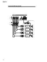
Page 46: ...Q P9 Connecting the RCA Input Amplifier Tweeter Mid range Woofer Subwoofer White White Red Red Power Amplifier Power Amplifier Power Amplifier Power Amplifier For system remote control Blue white Blue white ...

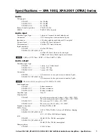
Page 47: ...oct Gain 0 dB 24 dB 0 5 dB MID HPF frequency 200 Hz 10 kHz 1 3 oct LPF frequency 2 kHz 20 kHz 1 3 oct Gain 0 dB 24 dB 0 5 dB HIGH HPF frequency 1 6 kHz 20 kHz 1 3 oct LPF frequency 8 kHz 20 kHz 1 3 oct Gain 0 dB 24 dB 0 5 dB Slope PASS 6 12 18 24 30 36 dB oct PASS no pass HPF High channel Phase NORMAL REVERSE Time alignment 0 134 in 0 67 in Position adjustment DISTANCE 0 134 in 0 67 in Level 0 30 ...

Page 48: ... 250 Hz 10 kHz 1 3 oct Gain 0 dB 24 dB 0 5 dB MID HPF frequency 200 Hz 10 kHz 1 3 oct LPF frequency 2 kHz 20 kHz 1 3 oct Gain 0 dB 24 dB 0 5 dB HIGH HPF frequency 1 6 kHz 20 kHz 1 3 oct LPF frequency 8 kHz 20 kHz 1 3 oct Gain 0 dB 24 dB 0 5 dB Slope PASS 6 12 18 24 30 36 dB oct PASS no pass HPF High channel Phase NORMAL REVERSE Time alignment 0 340 cm 1 7 cm Position adjustment DISTANCE 0 340 cm 1...

Reviews: