background image

DVR-220-S

72

1

2

3

4

1

2

3

4

C

D

F

A

B

E

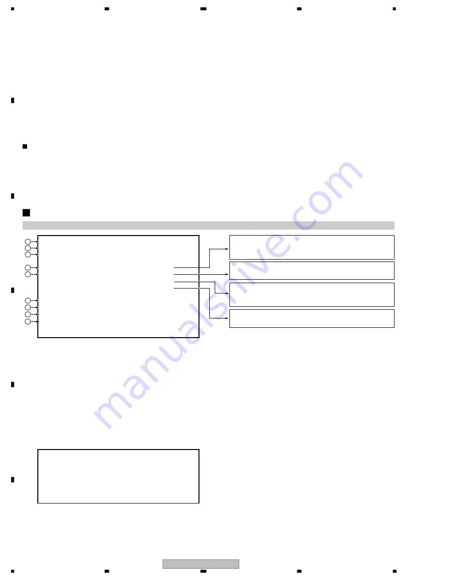
7.1.4  SERVICE MODE

For service operations, use the GGF1381 remote control unit for service.
The Service-mode screens consist of nine mode screens, which are classified into such rough categories as recording system and VR 
playback system, and their subscreens.

• How to enter Service mode :

Press the ESC then DISP keys in turn while no GUI is displayed. The first screen (version 
information, etc.) shown below is displayed.

• How to exit Service mode

:

Press the ESC key.

• How to advance to the next Service-mode screen

:

While the first screen is displayed, press directly one of the keys 1-9. For service, use the 
keys 2, 4 or 5, as shown below.

• How to advance to a subscreen within the same Service-mode screen

:

Press the DIG/ANA key. Pressing the DIG/ANA key repeatedly will change the subscreens 
within the same Service-mode screen cyclically.

Note:

After entering one of the Service-mode screens, if you wish to shift to another Service-mode screen, exit Service mode first, 
then reenter Service mode and select your desired Service-mode screen.

DVR-220/KU/CA
   VERSION

:1.07

SYSCON

: RELEASE_44

Rev      :1.3599.2.2

$

TUFLCON

: 1.22

MASK

OK  

DRIVE

:  DVD-RW DVR-107R

OK

                         1.03

OK

                         DADL000219WL

OK   

DEVICE

: PRISM-PLUS

REGION

: 1

C

:

∗ ∗ ∗ ∗ ∗ ∗ ∗ ∗ ∗

    FLASH

: 32M

Description of Each Service-mode screen

• Subscreen: Result of error-rate measurement

ERR RATE

: x.xe-x/

1
2

4
5

6
7
8

9

3

OK

:

OK (proper combination)

NG+ :

Version of the tuner microcomputer too advanced

NG– :

Version of the tuner microcomputer too old

OK

:

OK (proper combination)

NG+ :

Version of the drive too advanced

NG– :

Version of the drive too old

OK

:

Serial No. of the drive already registered

NG

:

Serial No. of the drive not registered

OK

:

OK (proper drive)

NG

:

NG (improper drive)

1

Model name/destination

2

Version of the recorder software

3

Revision No. of the system-control computer software 
(Edition administration No. [from top to bottom, common 
software, firmware, application software])

4

Version No. of the tuner microcomputer, Mask or 
Flash

      Result of the combination ckeck with system u-com

5

Information on the built-in drive
(Model name, version No., model type, serial No.)

6

Version No. of PRISM

7

Region No.

8

CPRM data (CPRM key No.)

9

FLASH ROM information

While the first screen shown above is displayed, press the DIG/ANA key to enter the subscreen shown below.

Note: 

Each time the DIG/ANA key is pressed, the display changes between the first screen and its subscreen.

Note:

Be sure to start playback after displaying this subscreen 
to calculate the error rate.

1. First screen (version information, etc.)

During playback in VR mode, the average error rate of the past 10 VOBUs is displayed, and during playback in DVD-Video or 
Video mode, the average error rate of the past 256 sectors is displayed. During playback in VR mode, the rotation rate of the 
drive (/: normal speed, no display = double speed) is also displayed.

The Service-mode screens to be used for service are as follows:

1 = First screen: Version information, etc.
2 = Second screen: ATA/ATAPI debug screen (Writer data)
4 = Fourth screen: Error log for the VR recording system
5 = Fifth screen: Error log for the VR playback system

(

*

1)

(

*

2)

(

*

3)

(

*

4)

(

*

1–

*

4 : Refer to next page)

Summary of Contents for DVR-220-S

Page 1: ...OWING MODEL S AND TYPE S Model Type Power Requirement Region No Serial No Please confirm 3rd 4th alphabetical letters DVR 220 S KU CA AC120V 1 DVR 220 S KUXU CA AC120V 1 PG DVR 220 S KUXQ CA AC120V 1 CP DVR 225 S KUXU CA AC120V 1 PG When servicing this model some service procedures may reset the settings that customer set to the factory default settings Make sure to explain this to the customer In...

Page 2: ...are often not evident from visual inspection nor the protection afforded by them necessarily can be obtained by using replacement components rated for voltage wattage etc Replacement parts which have these special safety characteristics are identified in this Service Manual Electrical components having such features are identified by marking with a on the schematics and on the parts list in this S...

Page 3: ...S SHOULD BE DONE BY A SPECIALLY INSTRUCTED PERSON LABEL CHECK PU LL OP EN STA ND BY ON DV D HD D OP EN CLO SE RE C ON E TO UC H CO PY Î CLAMP signals for detecting the loading state are detected by the drive CPUs and the design prevents laser diode oscillation when the CLAMP signal turns OFF In normal operation if no disc is clamped the laser diode oscillation is disabled However the interlock doe...

Page 4: ...es 5 Lubricants glues and replacement parts Appropriately applying grease or glue can maintain the product performances But improper lubrication or applying glue may lead to failures or troubles in the product By following the instructions in this manual be sure to apply the prescribed grease or glue to proper portions by the appropriate amount For replacement parts or tools the prescribed ones sh...

Page 5: ...3 9 MAIN ASSY 4 4 36 3 10 FLKY KIRB and FRJB ASSYS 38 3 11 POWER SUPPLY UNIT 40 3 12 WAVE FORMS 41 4 PCB CONNECTION DIAGRAM 43 4 1 TUNB ASSY 44 4 2 JCKB ASSY 46 4 3 MAIN ASSY 50 4 4 FLKY KIRB and FRJB ASSYS 54 4 5 POWER SUPPLY UNIT 58 5 PCB PARTS LIST 60 6 ADJUSTMENT 64 6 1 TUNB ASSY ADJUSTMENT 64 6 2 MAIN ASSY ADJUSTMENT 65 7 GENERAL INFORMATION 66 7 1 DIAGNOSIS 66 7 1 1 CPRM ID NUMBER AND DATA S...

Page 6: ...ck Quartz lock 12 hour digital display Power off memory Approx 5 years after manufacture Input Output VHF UHF antenna input output terminal VHF UHF set 75 F shape connector Video input Input 1 3 rear 2 front Input level 1Vp p 75 Jacks RCA jack Video output Output 1 2 Output level 1Vp p 75 Jacks RCA jack S Video input Input 1 3 rear 2 front Y luminance Input level 1Vp p 75 C color Input level 286 m...

Page 7: ...A and KUXQ CA types DVR 225 S KUXU CA Dry cell batteries 2 AA R6P Red White Yellow DVD RECORDER STANDBY ON OPEN CLOSE AUDIO SUBTITLE ANGLE PLAYMODE TOP MENU MENU RETURN DISC NAVIGATOR PLAY LIST HOME MENU INPUT SELECT ABC DEF GHI JKL MNO PQRS TUV WXYZ CLEAR ENTER CHANNEL PAUSE STOP OK SKIP CM BACK REV SCAN PLAY FWD SCAN DISC HISTORY NAVI MARK CASE SELECTION CHP MARK EASY TIMER INPUT SELECT DISPLAY ...

Page 8: ...cal designation Screws adjacent to mark on product are used for disassembly For the applying amount of lubricants or glue follow the instructions in this manual In the case of no amount instructions apply as you think it appropriate NOTES 9 7 8 10 12 13 15 14 10 4 6 2 5 DVR 220 S Only 11 3 1 Note When re packaging DVR 220 S models be sure to pack it with the front side of the unit properly oriente...

Page 9: ...HL1051 11 Mirror Sheet VHL1006 12 IM Holder See Contrast table 2 13 Front Pad See Contrast table 2 14 Rear Pad See Contrast table 2 15 Packing Case See Contrast table 2 Mark No Description Part No Mark No Symbol and Description DVR 220 S KU CA DVR 220 S KUXU CA DVR 220 S KUXQ CA DVR 225 S KUXU CA 1 Power Cable ADG7021 ADG7075 ADG7075 ADG7075 2 Audio Video Cable XDE3049 VDE1077 VDE1077 VDE1077 NSP ...

Page 10: ...NTACT SIDE B C F H A B 42 42 45 50 50 50 50 50 50 22 50 50 50 50 34 3 17 12 13 14 19 36 48 48 46 28 8 2 1 48 49 49 50 26 37 11 50 50 49 49 50 21 20 39 Refer to 2 3 FRONT PANEL SECTION 38 40 33 18 50 50 50 24 4 25 16 50 50 50 10 9 37 30 23 27 42 42 42 7 6 35 50 45 29 50 50 41 50 31 32 47 47 Lithium Battery CR2032 ...

Page 11: ... VEC2413 25 FFC Protector VEC2436 26 Gasket 20 x 8T VEC2437 27 Gasket Sheet 2 VEC2440 28 Rear Panel See Contrast table 2 29 Bonnet Case S VXX2925 NSP 30 Bonnet Angle VNE2335 NSP 31 Writer Stay L VNE2336 NSP 32 Writer Stay R VNE2337 NSP 33 PCB Base VNE2339 NSP 34 Heatsink VNH1070 35 SYPS Cover VNK5426 NSP 36 Base Chassis Assy VXA2681 NSP 37 Binder BK 1 ZCA BK1 38 DVD RW Badge VAM1139 39 Tray Sheet ...

Page 12: ...E NON CONTACT SIDE D E 3 2 4 18 6 8 16 5 10 1 21 21 12 9 2 3 9 3 3 9 1 3 13 11 7 21 21 14 19 21 21 17 Note 20 15 Note When replacing the jack door first fully open it If the jack door is not fully open during replacement it may unexpectedly fall out after being replaced ...

Page 13: ...g VNK5425 NSP 11 Sub Panel VNK5442 NSP 12 Power Key VNK5539 NSP 13 IR Window VNK5446 NSP 14 Sensormatic Seal See Contrast table 2 NSP 15 FL Lens See Contrast table 2 NSP 16 Front Panel VNK5492 17 Jack Door VNK5494 18 Rubber Foot VEB1349 19 Drive Sheet VEC2345 20 Panel Sheet VEC2446 21 Screw BPZ30P080FTC Mark No Description Part No Mark No Symbol and Description DVR 220 S KU CA DVR 220 S KUXU CA DV...

Page 14: ... 11 14 12 19 27 17 15 13 79 77 75 7 5 3 LPF 1 Chip Sysytem Codec Audio MPX Decoder Audio Selector with Electirc ATT 7 21 JA1302 JA1301 VIN2 YIN2 CIN2 2 LIN2 INPUT1 INPUT3 VIDEO Y C L R PICKUP ASSY Y C Y C JA601 VIDEO Y C L R VIN1 LIN1 LIN3 VIN3 YIN1 YIN3 M 40P ATAPI DVD VR DVD Video DVD VR DVD Video CD Digital CD Digital CN4401 1 CN201 2P CN703 2P CN101 45P 8 CIN1 CIN3 CN501 CN502 12P 33 39 A B C ...

Page 15: ... 2 2 27 29 25 23 21 L OUT 17 17 SPDIF 1 1 3 2 1 IC3251 1 2 UPC4570G2 Cb Cb Cr Cr Y G Y G Y C V Tuner U com JA651 OPTICAL AC 3 PCM DIGITAL AUDIO OUT LINE OUT 1 VIDEO JA702 Y C Y C VIDEO L R L R Y G JA701 R ch is same as L ch Cb Cr COMPONENT VIDEO OUT LINE OUT 2 32P CN2001 9 5 7 Master Clock Freerun 48KHz 20Bit JCKB ASSY 3 3 3 3 B ENC SDRAM 128Mbit IC1201 DEC SDRAM 128Mbit 53 51 45 43 41 56 60 58 63...

Page 16: ...Y C V Y C S S S L R L R L R JA702 IC701 LA73033 Video Selector Video Driver 2 2 IC701 LA73033 Video Selector Video Driver 1 2 u com SCL SDA YVSEL SWSTBY u com R L V Y U V U V C SYNC Sync Sepa LPF LPF LPF 27 25 36 51 53 5 45 60 56 58 63 65 68 41 43 26 TUNB ASSY VWV2010 A JCKB ASSY VWV2027 B FRJB ASSY VWV2004 F CN1301 CN705 CN402 CN401 CN301 CN451 4 10 12 2 6 8 8 6 12 2 JA701 JA651 Component OUT Opt...

Page 17: ...BR24L32F W IC203 Real Time Clock RS5C372A U com I F Y 9 10 11 12 13 14 15 3 4 5 6 7 8 16 17 18 19 20 21 22 23 24 25 26 27 28 29 30 31 32 C Y G Cb B Cr R R L SELC CN703 from DRIVE SELV Y SELR SELL 2 D E SYNCAFT Q514 IC1001 Q104 IC204 BT201 X201 Reset IC PST3265 IC201 IC1201 S1201 S1203 S1001 S1009 SR In JA201 FL Display V1001 SYNC IC701 MUTE IC451 TUON ASCK SST to M SSM to TSIS HST to M HSM to TSYS...

Page 18: ... IC1201 DEC SDRAM W986416DH 6 VYW2179 DCLK0 ECLK0 CD D OUT D OUT AGC ACC IC3201 PCM1742KE DAC IC3101 A D AK5381VT ADCCLKO IC3403 AUDIO LR OUT AUDIO LR IN VIDEO Y C Yp Cb Cr OUT IC3251 VIDEO Y C IN CN2001 CN3001 TO TUNER u COM CN1901 SERIAL IC1001 M65673WG 1 Chip System Codec MPEG2 PS Encode AC 3 Linear PCM Audio Encode 2ch ATA ATAPI Interface MPEG2 PS Decode AC 3 MPEG1 Linear PCM Audio Decode MAIN...

Page 19: ... E HOST BUS IC1101 CPU SDRAM K4S281632E TC75 HCLK0 IC3301 SRC SRC O SRC I IC4205 TC7WHU04FU SM5950AM Play Mster clock IC4206 AMCLK2 IC3402 PLL IC 27M 24M VMCLKI AMCLK1 33M 36M 33 36M X4102 VSS1195 VCXO Input Mster clock ADMCLKI 27M SM8707KV ...

Page 20: ...04 13P V 28V VEE 1 2 3 14 18 19 18 17 6 V 5VO V 5VI V 13SW CN701 32P CN2001 32P 32 32 V 5VO CN702 24P CN3001 24P 21 23 21 23 V 5VI V 13SW CN301 19P 13 11 7 9 V 6E V 37E FLDC FLDC NC V 5E V 5E CN1001 19P CN2005 19P V 6E V 13SW V 6SW IC101 5V REG V 6E V 5M V 5E IC102 3 3V REG V1001 FL TUBE IC1001 FL Driver V 6E V 6SW V 6E V 3_3E V 5VO V 13V V 4V V 4V V 6V V 2R5V V 5VO Q4000 V 12A V 5VI V 5RP IC103 9...

Page 21: ...DVR 220 S 21 5 6 7 8 5 6 7 8 C D F A B E ...

Page 22: ...2 1 2 3 4 1 2 3 4 C D F A B E 3 2 OVERALL WIRING DIAGRAM POWER SUPPLY UNIT VWR1378 G TUNB ASSY VWV2010 A MAIN ASSY VWV2007 C 1 4 C 4 4 C JCKB ASSY VWV2027 B 1 2 B 2 2 B ADG7075 OTHERS ADG7021 DVR 220 S KU CA ONLY ...

Page 23: ...UNDER LINE 3 VKB1150 When ordering service parts be sure to refer to EXPLODED VIEWS and PARTS LIST or PCB PARTS LIST The mark found on some component parts indicates the importance of the safety factor of the part Therefore when replacing be sure to use parts of identical designation The power supply is shown with the marked box VNF1129 ...

Page 24: ...DVR 220 S 24 1 2 3 4 1 2 3 4 C D F A B E 3 3 TUNB ASSY A TUNB ASSY VWV2010 A T T T T T T T T T ...

Page 25: ...DVR 220 S 25 5 6 7 8 5 6 7 8 C D F A B E A CN401 B 2 2 CN402 B 2 2 Video Signal Route TUNER T Audio Signal Route TUNER Audio Signal Route L ch T T T T ...

Page 26: ... 1 2 3 4 1 2 3 4 C D F A B E 3 4 JCKB ASSY 1 2 B 1 2 B 1 2 CN201 B 2 2 B 2 2 B 2 2 JCKB ASSY VWV2027 G 2 2 B 2 2 B Video Signal Route Y Video Signal Route Y Video Signal Route C Audio Signal Route L ch C Y Y C C 1 ...

Page 27: ...DVR 220 S 27 5 6 7 8 5 6 7 8 C D F A B E B 1 2 B 2 2 B 2 2 CN1001 D PEG034B EEPROM TUFL u com ...

Page 28: ... 2 2 JCKB ASSY VWV2027 CN301 A CN451 A CN1301 F B 1 2 B 1 2 B 1 2 Video Signal Route TUNER Video Signal Route T Video Signal Route Y Audio Signal Route L ch Y Audio Signal Route DIGITAL D Video Signal Route C C Y C Video Signal Route Cb Cb Video Signal Route Cr Cr T 2 ...

Page 29: ...S 29 5 6 7 8 5 6 7 8 C D F A B E B 2 2 B 1 2 CN3001 C 3 4 CN2001 C 2 4 From DRIVE ASSY R7R T Y Y Cr Cb Y Y C C Y D D D D D C Y Cb Cr Y Y Y C 5 6 13 12 15 14 11 18 17 16 9 8 7 3 4 10 Video Selector Video Driver ...

Page 30: ...DVR 220 S 30 1 2 3 4 1 2 3 4 C D F A B E 3 6 MAIN ASSY 1 4 C 1 4 4 4 C 2 4 4 4 C 2 4 C 2 4 C 2 4 C 2 4 4 4 C 3 4 C 3 4 C M65673WG A 4 4 C D D AT ...

Page 31: ...DVR 220 S 31 5 6 7 8 5 6 7 8 C D F A B E C 1 4 C 1 4 MAIN ASSY VWV2007 2 4 C VYW2179 D ATA Data Signal Route Audio Signal Route DIGITAL Audio Signal Route L ch AT FLASH ROM ...

Page 32: ...DVR 220 S 32 1 2 3 4 1 2 3 4 C D F A B E 3 7 MAIN ASSY 2 4 C 2 4 C 2 4 C 1 4 C 1 4 C 1 4 C 1 4 C 1 4 MAIN ASSY VWV2007 ...

Page 33: ...DVR 220 S 33 5 6 7 8 5 6 7 8 C D F A B E C 2 4 C 1 4 C 1 4 C 1 4 C 3 4 CN701 B 2 2 C 3 4 C 3 4 Audio Signal Route L ch 7 17 16 9 10 8 13 12 11 4 15 3 5 6 ...

Page 34: ...DVR 220 S 34 1 2 3 4 1 2 3 4 C D F A B E 3 8 MAIN ASSY 3 4 C 3 4 CN702 B 2 2 C 2 4 C 2 4 C 4 4 C 4 4 C 4 4 C 2 4 C 1 4 C 4 4 C 1 4 VKN1814 18 14 D D D D D D ...

Page 35: ...DVR 220 S 35 5 6 7 8 5 6 7 8 C D F A B E C 3 4 C 3 4 MAIN ASSY VWV2007 C 2 4 C 1 4 C 2 4 C 2 4 C 1 4 D Audio Signal Route DIGITAL Audio Signal Route L ch ...

Page 36: ...DVR 220 S 36 1 2 3 4 1 2 3 4 C D F A B E 3 9 MAIN ASSY 4 4 C 4 4 CN202 G C 4 4 MAIN ASSY VWV2007 C 3 4 C 3 4 C 1 4 C 1 4 C 3 4 C 1 4 2 4 C 1 4 2 4 MM1603DP 1 2 ...

Page 37: ...DVR 220 S 37 5 6 7 8 5 6 7 8 C D F A B E C 4 4 To DRIVE ASSY R7R C 1 4 ATAPI BUS AT AT ATA Data Signal Route ...

Page 38: ...DVR 220 S 38 1 2 3 4 1 2 3 4 C D F A B E 3 10 FLKY KIRB and FRJB ASSYS D CN201 B 1 2 FLKY ASSY VWG2489 D 1 0 ...

Page 39: ...VWV2004 F Video Signal Route C Audio Signal Route L ch C C C Video Signal Route Y Y Y Y Video Signal Route INPUT 2 SWITCHES S1001 0 OPEN CLOSE S1002 REC STOP S1004 7 STOP S1005 REC S1006 REC MODE S1007 S1008 S1009 3 PLAY SWITCHES S1201 STANDBY ON S1202 DISC HISTORY S1203 DISC NAVIGATOR 100 ...

Page 40: ...3 4 D23 N L F1 VS1 C1 C4 C2 L1 R1 CN101 C3 D1 D2 D3 D4 C5 TH1 R2 R3 VS2 VS3 AR1 C38 11 15 14 13 17 18 16 4 1 2 3 5 6 7 8 L5 R41 R42 Q10 Q14 C29 Q11 Q12 C31 R54 R43 D19 C30 D21 D20 C27 C28 D22 R44 T2 R47 R48 R52 R53 R55 R56 Q17 R58 R57 C43 D28 3 10 12 R59 R60 C21 C45 C8 R46 C37 C46 CP4 D38 R64 R65 R66 R67 IC6 C47 Q18 SW6V GND VR1 C35 R37 R36 IC3 C48 Last No T2 L6 IC7 D41 Q20 C66 R79 C53 R72 R74 R75...

Page 41: ...unction DVD play V 500mV div H 10µsec div 11 CN701 pin 5 ALTtoM Function DVD play V 1V div H 200µsec div 12 CN701 pin 17 ALMtoT Function DVD play V 2V div H 200µsec div 13 CN701 pin 25 YGMtoT Function DVD play V 500mV div H 10µsec div 10 JA702 pin 4 COUT Function DVD play V 500mV div H 10µsec div 16 IC701 pin 60 PYRSCOUT Function DVD play V 500mV div H 10µsec div 15 CN701 pin 21 CRRMtoT Function D...

Page 42: ...1 Cr Out V 500mV div H 10µsec div Function PLAY 11 CN2001 pin 29 Y Out V 500mV div H 10µsec div Function PLAY 12 CN2001 pin 27 C Out V 500mV div H 10µsec div Function PLAY 13 CN2001 pin 25 Y Out V 500mV div H 10µsec div Function PLAY 14 CN3001 pin 13 PCMAIN V 1V div H 400nsec div Function PLAY 15 CN2001 pin 9 SEL Y V V 500mV div H 10µsec div Function L1 16 CN2001 pin 7 SEL C V 500mV div H 10µsec d...

Page 43: ...ed on this PCB include all necessary parts for several destinations For further information for respective destinations be sure to check with the schematic diagram 4 View point of PCB diagrams Symbol In PCB Diagrams Symbol In Schematic Diagrams Part Name B C E D D G G S S B C E B C E D G S B C E B C E B C E Transistor Transistor with resistor Field effect transistor Resistor array 3 terminal regul...

Page 44: ... L303 JA301 C316 Q306 C318 CN301 C461 C451 VR451 VR452 R454 R453 R455 C459 C453 C462 C456 C458 C460 R463 VR453 C465 R467 R466 R468 C473 Q451 CN451 C467 C468 C471 C472 C474 R471 R326 VNP1963 A LF SEPA WIDE INPUT LAVEL ADJAST SPECTRUM SEPA ADJAST ADJAST FC ICT V 9 V 9 GND V 5TU Q451 Q306 Q304 Q302 Q301 VWV or GND PC G Link TUNB PYKC F4X C2 B E E2 B2 C R NP 19 1 NP 13 1 SIDE A SIDE A A A TUNB ASSY A ...

Page 45: ...64 R469 C466 R465 C464 C463 R472 R473 R474 R475 C469 R476 R477 C470 R470 R479 R478 C475 C476 C477 IC452 R327 R481 C478 L4 UVIN VWV2034 UVIN LF VIDEO NC SIFtoONTA V 9 GND GND V 6E R4 IC452 IC451 Q307 Q305 Q303 SD STID BT 33V SDA V 6E G Link V 37E V 5 T U or UVA_IN AFT GND AUDIO IF MB 5V BP 5V MUTE SIF ADRS SCL TUON VWV2016 SU SAPID AFT V 6E UV_LIN L4 AGC SDA UV_LIN MIONTA SCL UV_RIN R4 FOMOI AGC 28...

Page 46: ...240 IC204 L201 R240 Q202 R111 C206 R268 R178 R179 R172 R183 D103 X201 R180 R292 R173 L171 Q173 Q171 R176 R174 Q172 C251 C252 R175 R185 R293 R270 R200 R184 R299 R294 X204 BT202 R265 R264 CN11 C141 R300 R308 CN12 R447 R448 R454 R301 CN13 V 5M SCL SDA SIDE CONTACT VNP1961 A V 5M AGC AFT L R V C Y SDET2 GND GND GND GND GND GND GND FLSTB FLDATA FLPON GND GND KEY1 KEY2 DVD V 5E GND V 13 FLCLK NC IR HDD ...

Page 47: ... X401 R180 Q712 Q171 C751 C251 C252 R562 R563 C748 R294 R565 CN403 R780 R564 R770 R771 R772 R773 R774 Q771 R264 IC501 C501 C502 C141 R301 R785 R784 R783 R781 R782 C503 V 5M Y_TtoM YtoM CtoM Cr NC RfromM Y2 Y RtoM Cr Cb Y CSYNC AFT SD STID MIONTA GND NC C LtoM FOMOI LfromM Cb VWV2029 Y GND GND GND L GND NC V 9 P_ON GND NC AGCCTL SCL R SD SAP GND LM GND GND AGC SDA MUTE TUON V 6E V 5VO V 37E SIF JUS...

Page 48: ...47 C605 IC601 C613 R609 R738 R733 R708 R710 R709 R713 R417 R416 R412 R411 R409 D401 R410 C127 C134 C124 C122 C120 D713 R408 R405 R404 R501 R520 C514 C131 C518 C519 Q505 R445 R446 R775 R444 R443 R441 R442 R760 R761 R306 R307 IC101 C108 R776 C755 C754 C753 R452 C761 C762 C763 C764 C768 C767 C766 C765 C66 R778 R779 D105 C771 C772 C773 C770 C769 C758 C757 C756 19 AGC SDA RfromM LfromM Cr AGCCTL Y C Rt...

Page 49: ... R238 L205 R241 R260 R267 R295 R182 C171 R181 R171 D104 R113 R177 R291 L284 R186 R441 R442 R112 L206 L208 C253 R305 R306 R307 R298 R297 R296 IC101 C108 R449 R450 R451 R453 C234 Q408 Q409 Q410 Q411 D601 D602 D603 D604 D605 D606 D718 D719 D720 L207 C655 C654 C661 C660 C659 C658 C657 C656 D105 C772 773 C770 C769 DLCE 1 FANPWM P_CONT JUST SYNCAFT GND SDET2 GND Y GND C GND V GND R GND L GND GND GND FLP...

Page 50: ... 7 1 7 1 C2301 Q2301 Q2201 Q2222 Q2103 TP14 C2101 C1039 C1049 C1036 C1038 C1035 C1029 C1030 C1026 C1024 C1023 C1022 C1021 C1048 C1047 C1012 C1052 C1051 C1005 C1006 C2222 C2209 C2202 C2306 R1008 R1004 D4201 R4209 R4208 R4207 R3104 D4202 6 1 8 1 C2210 R4205 R1080 R4201 C4201 C4202 R5222 R5223 R2204 R2239 R2221 R2227 R2205 R2203 R2209 8 2 R4304 8 2 R4303 8 2 R4302 8 2 R1048 8 2 R1045 8 2 R1043 VC4201...

Page 51: ...55 1 7 R4507 1 7 2 8 1 2 L1006 CN4501 C1059 12 13 IC3301 R3311 R1066 R3307 R3310 R1031 IC5204 8 2 7 1 R4510 8 7 8 2 7 1 R4509 C5321 1039 1049 1048 1047 052 C1051 C1005 C1006 R1008 R3104 R3103 3 1 C3102 C4027 C4018 F4001 F3403 C3301 F3401 L5508 L3301 C3403 1 24 R3313 R5298 R5297 R3306 R3305 R4530 R4531 R4534 R4537 R4541 R3407 R3403 R3405 R3406 R3309 D4001 IC4008 R3411 8 2 7 1 R4538 8 5 IC3403 2 D45...

Page 52: ...101 C5307 IC5321 5 4 IC4006 5 4 3 1 R5328 7 1 8 2 7 1 R4518 8 2 7 1 R4512 8 7 8 2 7 1 R1407 8 2 7 1 R1406 C1406 IC1401 R1402 R5324 R5329 R5264 C5323 C5325 C5328 C1408 C1407 R4533 R4528 R4527 TP4507 TP4509 TP4510 TP4511 TP4513 TP4517 TP4515 TP4514 TP4518 TP4519 TP4520 TP4512 TP4516 R5322 TP5003 C5324 L5321 3 1 IC5322 1 4 5 8 R4005 R4012 R3266 C4008 C4007 R3268 R1055 C1401 TP1 C5008 1 16 L1401 F3201...

Page 53: ...058 R1035 TP1017 TP1001 TP1004 TP1020 6 TP101 TP5211 TP5209 TP5210 TP5208 TP5207 TP5206 TP5205 TP100 R1069 1 7 2 8 8 2 7 1 R1054 7 1 27 C1109 C1111 R1064 R5264 R1105 R1060 07 R1063 R1062 R1061 R1093 R1119 TP1005 TP1006 TP1007 TP1008 TP1009 TP1042 L2501 C2506 IC2501 TP1901 R3268 8 7 R1051 C1207 C1202 1 54 C1102 R1055 R1070 R1081 TP1010 TP1036 TP1022 TP1062 TP1061 TP1065 TP1066 16 8 2 7 1 R1117 8 2 ...

Page 54: ...C MODE IR GND GND V 5FL DUBBI V 13SW FLSTB LED_DVD VWG2489 ONE TO VDD GND GND KEY2 ACP BS MODE OPEN CLOSE VWG2493 IR STOP VDD FLSTB LED CONTACT SIDE HDD KIRB ASSY VWG2490 CONTACT UPPER SIDE FLDC DVD PC V 5FL V 13SW FLDC ACP BS FL 28V CONTACT SIDE PLAY GND VWG LED_HDD PC REC STOP VWG2508 DVD H DISC NAVI S HDD H FL 28V V 5FL V 5FL GND GND ONE TO DISC HISTRY S POWER GND V 13SW VDD GND OPEN CLOSE REC ...

Page 55: ...1022 CN1301 W1302 W1019 W1006 W1027 W1005 S1007 S1006 S1008 W1303 MODE H REC MODE S DUBBING VDD ONE TOUCH L R MODE H C VWV2004 Rch S_DET VWV FRJB ASSY S Video Video Lch C VDD GND GND FLKY ASSY GND C FLDC GND VDD VDD ONE TOUCH GND GND GND GND GND J REC MODE S VDD DUBBING FC FLPON ACP BS 1 13 49 41 33 SIDE A F D FRJB ASSY F CN705 B CN1301 VNP1962 C ...

Page 56: ...09 R1031 Q1008 R1033 R1032 R1030 R1029 Q1007 R1010 R1012 R1016 R1015 R1011 R1009 C1006 Q1002 R1008 Q1001 I C R1309 C1305 D1303 R1306 D1301 C1304 C1302 D1304 V ACP BS R ONE TOUC DUBBING S_DET REC MODE S MODE H LF LF C Video Rch Lch S Video CONTACT VDD GND GND VDD GND C Y GND FLPON FLDC VDD GND B SIDE C L R L Q1009 Q1008 Q1007 Q1002 Q1001 IC1001 13 1 R 41 49 1 1 1 SIDE B D F FLKY ASSY D FRJB ASSY F ...

Page 57: ...S V 5FL V 13SW FLDATA GND FLDC KIRB ASSY REC REC STOP ONE TOUCH DUBBING IR HDD LED_HDD IR IR LED REC MODE S MODE H IR LED_DVD VWG2490 GND A B LED_HDD KEY1 GND V 13SW POWER KEY1_2 V 5FL LED_DVD IR LED_HDD LF DVD H DISC NAVI S HDD H DISC HISTRY S GND V 13SW FL 28V FLKY ASSY VWG2489 VDD KEY2 LED_DVD KEY2 V 5FL KEY1 FLDC C GND GND V 5FL V 5FL GND VWG2493 FLSTB FLPON GND VDD GND V 5E DVD GND LED_DVD D ...

Page 58: ...VR 220 S 58 1 2 3 4 1 2 3 4 C D F A B E 4 5 POWER SUPPLY UNIT SIDE A SIDE A G G POWER SUPPLY UNIT G AC IN CN101 DRIVE ASSY R7 CN203 CN202 CN4001 C CN104 B CN201 Q2 Q1 Q4 Q5 Q3 Q10 Q11 Q18 IC2 IC4 IC3 IC6 ...

Page 59: ...ELFUSE INC REMPLACER UN MODELE PAR LE FUSIBLE PAR INDENTIQUE EN INTENSITE CP1 TYPE NO 491002 MFD BY LITTELFUSE INC C53 R23 C47 C65 R20 R19 Q6 C32 C37 C36 C64 C35 C63 C46 R46 R18 C43 C30 R57 R31 R32 C56 C11 C66 R12 R10 IC1 R13 R9 R14 R78 Q19 Q20 R77 R76 R29 R33 Q17 R28 R41 Q14 R55 R54 R74 R21 C67 R27 R40 R38 R37 R36 R24 C66 C65 C62 C60 C59 Q7 R60 R59 R30 R72 R11 R15 C45 R16 C12 R79 R52 Q12 C31 R43 ...

Page 60: ...302 RN4903 Q306 UMF21N D301 1SS355 D302 UDZS33B COILS AND FILTERS L302 CHIP FERRITE BEAD CTF1399 L304 L305 CHIP BEAD VTL1081 L303 RADIAL INDUCTOR VTL1165 CAPACITORS C460 C474 CCSRCH681J50 C301 C303 C451 C467 CEAT100M50 C319 CEAT101M10 C453 CEAT101M16 C305 CEAT102M6R3 C462 CEAT4R7M50 C459 C473 CKSRYB103K50 C469 C470 CKSRYB105K10 C475 CKSRYB123K50 C311 CKSRYB222K50 C452 CKSRYB272K50 C458 C472 CKSRYB...

Page 61: ...0 CKSRYF104Z25 C752 C760 CKSRYF104Z25 C101 C209 C210 C212 C213 CKSRYF105Z10 C218 C219 C227 C231 C236 CKSRYF105Z10 RESISTORS R178 RS1 16S1501F R173 RS1 16S3901F R519 R526 R534 RS1 16S5600F R602 R605 R606 R615 R617 RS1 16S75R0F Mark No Description Part No R704 R715 R717 R718 RS1 16S75R0F R728 R730 R740 R743 R747 RS1 16S75R0F R757 R759 RS1 16S75R0F Other Resistors RS1 16S J OTHERS X201 CERAMIC RESONA...

Page 62: ...3105 C3108 C3202 C3203 C3205 CKSRYF104Z25 C3252 C3256 C4006 C4008 C4010 CKSRYF104Z25 C4012 C4013 C4017 C4021 CKSRYF104Z25 C4024 C4026 C4032 C4107 CKSRYF104Z25 C4202 C4203 C4209 CKSRYF104Z25 C1001 C1006 C1048 C1103 C1107 CKSRYF105Z10 C1203 C1205 C1209 C1303 C1306 CKSRYF105Z10 Mark No Description Part No C1309 C1403 C1405 C1409 CKSRYF105Z10 C3404 C3407 C4027 C4030 C4201 CKSRYF105Z10 C4401 C4501 CKSR...

Page 63: ... VSG1024 CAPACITORS C1204 CKSRYF104Z25 RESISTORS All Resistors RS1 16S J OTHERS IC1201 REMOTE RECEIVER UNIT RPM7140 H9 CN1201 CONNECTOR VKN1183 FFRJB ASSY CAPACITORS C1308 C1309 CCSRCH471J50 RESISTORS R1501 R1502 RS1 10S0R0J Other Resistors RS1 16S J OTHERS CN1301 FFC CONNECTOR 13P 52492 1320 JA1301 YC CONNECTOR VERTI VKB1190 JA1302 3P JACK VERTICAL VKB1206 KN1301 WRAPPING TERMINAL VNF1084 GPOWER ...

Page 64: ...me Adj Point Measurement Point Adjustment Value Adjustment State 1 Stereo Decoder ATT adjustment Input system adjustment Stereo Decoder Wideband adjustment Input system adjustment Stereo Decoder Spectral adjustment Input system adjustment VR453 VR451 VR452 5 4 3 2 1 19 1 13 1 R328 R325 R324 C328 L306 C327 KN300 C329 D301 U301 C326 Q301 R301 C304 C301 C302 R307 R306 C313 D302 C303 C309 Q302 C305 C3...

Page 65: ...3 C5225 C5222 C1044 C1045 C1017 C1018 C1019 C2103 C2102 TP4304 TP4305 TP4306 TP4307 TP1067 Q2312 Q2102 Q2101 Q2302 C5205 1 7 R5255 1 7 2 8 2 8 R4507 1 7 2 8 1 2 R2301 L1003 L1006 CN4501 C2204 C1059 12 13 IC3301 CN4301 R3311 R1066 R3307 R2233 R2235 R3310 R2107 R2210 R2201 R2202 R2304 R2307 R1031 IC5204 8 2 7 1 R4510 8 7 8 2 7 1 R4509 7 1 7 1 C2301 Q2301 Q2201 Q2222 Q2103 TP14 C5321 C2101 C1039 C104...

Page 66: ...ror rate measurement Video mode VR mode Second Screen ATA ATAPI debug screen Sub Screen 3 writer maintenance information of ATA ATAPI DEBUG OSD Sub Screen 4 ATA ATAPI DEBUG OSD_LD degradation judgement Fourth Screen VR recording error log Sub Screen 4 Error log for VR recording Fifth Screen Error log for VR playback Sub Screen 2 Error log for VR playback 7 1 5 ERROR RATE MEASUREMENT Only Video mod...

Page 67: ...correctly with the following procedure operations in the future may not be guaranteed You will find the ID number to be set on the ID label on the rear panel The Input is Necessary When How to Input the ID Number and ID Data Recorder s ID Number Setting ID Number CLEAR Exit Input ID Number 1 As number input is enabled when the unit enters the input mode input the 9 digit ID number The entered numb...

Page 68: ...t enters the ID number confirmation mode The set ID number is displayed on the screen and on the FL display permitting you to confirm it To exit this mode press CLEAR 1 Press ESC STEREO sequentially with an ID number already set and the unit enters the ID number confirmation mode Input the same number as the ID number you have set 1 2 2 3 2 3 Recorder s ID Number Setting ID Number 0 0 0 0 0 0 0 0 ...

Page 69: ... the power cable and plug it again Then restart the model setting The setting complete when OSD is disappeared 3 Unplug the power cable 4 Reset the recorder to all its factory settings 1 Make sure that the recorder is on 2 Press and hold STOP and press STANDBY ON key on the front panel The recorder turns off with all settings reset 5 Enter the Service Mode and then confirm the Model Name DVR 220 K...

Page 70: ...ting of the TUFLCON program only for the flash type TUFLCON microcomputers The TUFLCON program will not function properly if the power to the unit is forcibly shut off while the message DOWNLOAD 3 is displayed on the FL display during downloading If downloading of the programs from the disc or through serial communication becomes impossible replace the TUFLCON microcomputer 1 DISC DOWNLOAD METHOD ...

Page 71: ... above way 2 Turn on the PC and start the UFU exe 3 Select the Firmware file sz0 file 4 Turn the DVD recorder on and start the download program Target Device is connected is appeared on the screen 5 Select the Communication Speed Baud Rate a Base Speed 38 400 b Data Send Speed 115 200 6 START Even if you click START button sometimes Communication Error may come out one to twice and download may fa...

Page 72: ...microcomputer too old OK OK proper combination NG Version of the drive too advanced NG Version of the drive too old OK Serial No of the drive already registered NG Serial No of the drive not registered OK OK proper drive NG NG improper drive 1 Model name destination 2 Version of the recorder software 3 Revision No of the system control computer software Edition administration No from top to bottom...

Page 73: ...ace the TUFL µ com or JCKB ASSY 2 When TuFL µ com is FLASH type NG Download the firmware NG Download the firmware 2 NG NG improper drive Replace the correct Drive Assy 3 NG Version of the drive too advanced NG Version of the drive too old NG Download the firmware NG Download the firmware 4 NG Serial No of the drive not registered Check the part No and replace the correct Drive Assy When NG is disp...

Page 74: ... 6 3 0 0 0 OK 3 2 2 A 0 0 0 0 0 E 0 A 9 0 0 0 0 6 3 0 0 0 OK 3 2 2 A 0 0 0 0 0 E 1 0 C 0 0 0 0 6 3 0 0 0 OK 3 2 2 A 0 0 0 0 0 E 1 6 F 0 0 0 0 6 2 0 0 0 2 3 A 0 0 Subscreen 3 Writer mentenance information of ATA ATAPI DEBUG OSD A T A A T A P I Writer MaintenanceInfo Power ON 0 0 0 0 0 0 0 0 0 0 0 0 0 0 0 0 0 0 0 1 0 2 5 6 0 1 0 0 0 0 0 0 0 0 0 0 0 0 0 0 0 0 D V D 0 2 0 0 0 0 0 0 0 0 0 0 0 0 0 0 0 0...

Page 75: ...gher same standard as for the PC drive No disc inserted in the disc tray 1 2 DVD Degradation judgment of LD for DVD Regarded as NG when the value is 120 or higher same standard as for the PC drive No disc inserted in the disc tray 1 3 TMP Current temperature inside the Writer No disc inserted in the disc tray 1 4 ADJ Temperature approx 25 C inside the Writer during adjustment No disc inserted in t...

Page 76: ...ur minute second error data in simplified description RunFnc Ecl Rate R e c o r d i n g E r r o r H i s t o r y D i s p l a y 0 1 0 6 0 1 2 0 0 5 3 0 N o S y s H d r I N 0 1 0 6 0 2 0 0 2 2 1 0 W r i t e E r r o r 1 Notes For details on error messages see Table 2 Description of VR recording related errors The two error log screens can be switched by pressing the SPEED or SPEED key These subscreens...

Page 77: ...rs XX XXXXXXX These subscreens are not for service use 4 Fifth screen Error log for VR playback Notes For details on error messages see Table 1 Description of VR playback related errors If a VR playback related error is generated a problem in data reading from the disc may be suspected The possibility of a problem on the drive side is high Note The information on this screen is not stored in the m...

Page 78: ... c n I k s a t P P T r v O T t s 1 v R g n i d o c e d g n i t r a t s r e t f a y l e t a i d e m m i U B O V p o t e h t o t n o i t p u r r e t n i r o f g n i t i a w r o f t u o e m i T k s a t k c a b y a l p e s r e v e R r v O T n p O v R g n i d o c e d g n i t r a t s r e t f a y l e t a i d e m m i P O G n e p o e h t f o e r u t c i p B r o f g n i t i a w r o f t u o e m i T k s a t k...

Page 79: ...rr Reading failed ECC failed etc Abnormality in the drive hardware or firmware Drv Hard Err Mech No Res No response from the mechanical control computer Timeout waiting for drive operation Drv Timeout NWA Exhaust MKB reading error NWA surpassed and impossible to use General error of the drive MKB Invalid Drv Err Fail Repair Repair failed Because some data are invalid data cannot be written Althoug...

Page 80: ...BU Info NG Ourob Strm NG WaterMark Det No Video Disc Full No More Info No Permission No permission to write to the disc Limit Over Standard maximum limit exceeded Rec Pause No operation permitted during recording pause Invalid Param Protect Src Now Busy Invalid Disc The disc cannot be recognized Invalid UDF Invalid UDF content Invalid VMG Invalid TMVMG Unmatch Stamp Impossible to modify because of...

Page 81: ...or Error Message Description Non Err Normal Notes Any error message marked with is displayed RecErr on the Subscreen 1 of the fourth screen In a case of an error in the drive system scratches or dirt on a disc or a problem of the drive itself dirty pickup may be suspected Abbreviations ECC 4 byte Code for Error Correction UDF Universal Disc Format PCA Power Calibration Area OPC Optical Power Contr...

Page 82: ...ent ESC SIDEB V mode recording After recording for 10 seconds the unit starts playback while displaying the error rate DVD Video The error rate is automatically measured then the result will be displayed For details see 7 1 4 ERROR RATE MEASUREMENT 3 Settings for specific areas ESC CHP TIM Enters Adjustment mode for AVIO settings Settings are made for the selected input TUNER LINE For details see ...

Page 83: ...FL display and OSD 2 Only in a case in which the calculation of the average error rate fails the tray will open Changes of display Table 1 Video mode recording medium E R R O R R A T E E R R O R R A T E x x x x x E R x x E x E R x x E x E R R R A T E x x E x E R R R A T E x x E x O K Operation Display FL Display OSD On Screen Display ERROR RATE is displayed on the FL display for an instant DVD rec...

Page 84: ...ble 4 List of OK NG threshold values Recording Mode Judgment whether error rate measurement is finished or not Recording playback duration required for error rate measurement Video mode After playback of a certain amount of data Measurement of the 16 ECC blocks is performed 16 times then the grand sum is used for calculation of the error rate The capacity is as follows 16 ECC blocks 16 sectors 204...

Page 85: ...A picture from the tuner can be viewed using the semitransparent OSD display 1 Specific Channel Setting mode AVIO Specific Area Mode Ver Input tuner Sync AGC ON Threshold Normal V Sync Det Normal Std Det Normal HD Err Det Normal Individual setting state Input Channel 1CH Sync AGC Threshold V Sync Det Std Det HD Err Det When specific channel settings have NOT been made When specific channel setting...

Page 86: ...he value is fixed with no display of the value Auto Threshold Level 0 8 Default 0 Manual Threshold Level 0 8 Default 0 Pedestal Level 0 8 Default 0 CLEAR Initializes the setting of Specific Channel Setting mode Pressing the key resets the settings of Specific Channel Setting mode for that channel to the initial values Settings of General Setting mode are not affected PAUSE The specific setting dat...

Page 87: ...t Normal Std Det Normal HD Err Det Normal Individual setting state Sorry You can store only 12 channels for Specific Area mode With 12 channels having specific settings when the currently selected channel does not have specific settings 2 General Setting mode This mode can be entered only during recording playback stop In this mode each item and its current settings are displayed on the OSD The cu...

Page 88: ...ld level According to the setting of Threshold the values can be changed within the range mentioned below Normal The value is fixed with no display of the value Auto Threshold Level 0 8 Default 0 Manual Threshold Level 0 8 Default 0 Pedestal Level 0 8 Default 0 CLEAR Initializes the setting of General Setting mode Pressing the key resets all settings of General Setting mode to the initial values S...

Page 89: ...paused Function During Aging mode the following operations are repeated in the order shown below 1 The tray opens 2 The tray closes 3 Initialization 4 Recording for 60 minutes 5 Playback for 45 minutes 3 Initialization is performed according to the setting specified in DVD RW automatic initialization accessed by selecting Unit Setting then Option During Aging the number of loops is indicated on th...

Page 90: ...yed on FL display Key input and channel data transmitted to the system control computer and responding to instructions from it indication displayed on FL display and channel switching performed Firmware stored in Flash memory is developed in SD RAM expanding the compressed data Yes Is disc valid Yes Yes No No No Playback requested Yes Stop Tray Open Jumping to developed firmware Downloading throug...

Page 91: ...ess the 0 OPEN CLOSE button to close the tray 6 Press the STANDBY ON button to turn off the power Bonnet S and Tray panel 1 1 Unhook the four hooks 2 Remove the front panel section Front panel section 2 3 5 4 1 1 1 2 1 3 5 2 6 Tray panel Front panel section Tray long thin pole Emergency eject hole Jack door How to open the tray when the power cannot be on When the player cannot eject disc tray due...

Page 92: ...ctor 4 Remove the tape 5 Remove the DRIVE Assy R7R CN703 DRIVE Assy R7R DVD R RW WRITER 3 1 Remove the four screws 2 Stand the MAIN Assy MAIN Assy MAIN Assy 4 1 3 4 5 SYPS cover DRIVE Assy R7R 2 DRIVE Assy R7R JCKB Assy Tape 2 1 1 1 1 2 2 2 2 2 Note This photograph may show a different model However the method for disassembly is the same ...

Page 93: ...e chassis 2 Arrange the unit as shown in the photo below Caution Main IC IC1001 on the MAIN Assy generate heat to arround 80 degrees Be careful when works Diagnosis 5 JCKB Assy Front panel section B POWER SUPPLY Unit G FRJB Assy F TUNB Assy Insulation sheet A DRIVE Assy R7R MAIN Assy IC1001 C Diagnosis ...

Page 94: ...emoving the three screws with the bonnet angle 3 Remove the bottom cover by removing the four screws Front side Front side Cleaning the pickup lens Pickup lens SYPS cover Bonnet angle Front bezel Hook Writer stay L Writer stay R Bottom cover Top cover Bonnet angle Before shipping out the product be sure to clean the following positions by using the prescribed cleaning tools Cleaning liquid GEM1004...

Page 95: ...SLICEON pin 19 P82 INT0 XINTRA I Alarm interval interruption for HDD Model for HDD Model 20 P81 TA4in LED HDD O H 21 P80 TA4out LED DVD O 22 P77 TA3in NC O 23 P76 TA3out FANPWM O FAN power control H 24 P75 TA2in JOGB I Phase VOL input 25 P74 TA2out NC O 26 P73 CTS2 RTS2 TA1in IICRST O 27 P72 CLK2 TA1out AVLINKOUT O 28 P71 RxD2 SCL TA0in TB5in SCL I O I2C communication clock 29 P70 TxD2 SDA TA0out ...

Page 96: ...ication line DATA 52 P51 WRH BHE VOLCLK O Communication line CLK 53 P50 WRL WR DLCE I Signal for serial I O mode selection 54 P47 CS3 S1 O 55 P46 CS2 LET O Letterbox signal add H 56 P45 CS1 SQU O Squeeze signal add 57 P44 CS0 BLANK I 58 P43 A19 XTHROU O 59 P42 A18 NC O 60 P41 A17 NC O 61 P40 A16 SWVION O Independent source SW for video I O output circuit H 62 P37 A15 SWSTBY O Standby mode of video...

Page 97: ...ower ON H 96 P107 AN7 KI3 MODEL1 A D IN Input for destination judgment 97 P106 AN6 KI2 MODEL2 A D IN Input for destination judgment 98 P105 AN5 KI1 AGC A D IN Field intensity detection 99 P104 AN4 KI0 FUNC A D IN 100 P103 AN3 KEY2 A D IN Main unit key input 101 P102 AN2 KEY1 A D IN Main unit key input 102 P101 AN1 NC 103 Avss GND 104 P100 AN0 AFT A D IN AFT voltage input 105 VREF VREF 106 AVcc AVC...

Page 98: ...t clock input Synchronize with this clock and input and output data from a SDA terminal Exceed VDD and can input to 6V 3 SDA I O Serial input and output Synchronize with SCL and input and output writing data or readout data Exceed VDD and can input to 6V Nch open drain output in the output 4 VSS Ground pin 5 INTRA O Interruption output A Cycled interrupt for CPU or output alarm interruption ALARM_...

Page 99: ...8 R2 4 TEST Pin for electronic volume test Set to VSS electric potential 19 R3 5 LOUT Volume and equalizer output pin 20 R4 6 LBASS2 Capacitor and resistor connection pins for bus bandpass filter 21 RSELO Input selector output pin 7 LBASS1 22 RIN Volume and equalizer input pin 8 LTRE Capacitor connection pin for treble bandpass filter 23 RTRE Capacitor connection pin for treble bandpass filter 9 L...

Page 100: ...DVR 220 S 100 1 2 3 4 1 2 3 4 C D F A B E Video selector and Video driver LA73033M JCKB ASSY IC701 Block Diagram ...

Page 101: ...ge output bias voltage of VA 2 and ADC input 5 AGND Analog ground 6 VA Analog power supply 4 5V to 5 5V 7 VD Digital power supply 2 7 to 5 5V fs 4k to 48kHz 3 0 to 5 5V fs 48k to 96kHz 8 DGND Digital ground 9 SDTO O Audio serial data output outputs L in the power down mode 10 LRCK I O Channel clock I O outputs L by master mode in the power down mode 11 MCLK I Master clock input 12 SCLK I O Audio s...

Page 102: ...tage detection 3 NC Not connected 4 VSS VSS PST3428U MAIN ASSY IC4003 Pin Function Pin Arrangement Top view Block Diagram VDD OUT OUT 1 Vref 2 1 GND 4 VDD 2 4 GND 3 NC No Pin Name Function 1 OUT Reset signal output 2 VDD Power supply voltage detection 3 NC Not connected 4 GND Ground Reset IC PST3809U MAIN ASSY IC4005 Pin Function Pin Arrangement Top view Block Diagram ...

Page 103: ...er 5V tolerant pull down PDO04CDG Output buffer 4mA PDO08CDG Output buffer 8mA PDO0204DGZ Output buffer 2 4mA PDO0406DSGZ Output buffer 4 6mA For SDRAM IF PDO0406DSGZ 2 Output buffer 8 12mA For SDRAM IF PDT0204DGZ 3 state output buffer 2 4mA PDB04DGZ Bidirectional buffer 4mA PDB08DGZ Bidirectional buffer 8mA PDB0204DGZ Bidirectional buffer 2 4mA PDB0406DSGZ Bidirectional buffer 4 6mA For SDRAM IF ...

Page 104: ...D GND GND GND VDD3 TCK TDI TDO TMS PLLON AT2MODE AT2CS 0 AT2CS 1 AT2ADR 0 AT2ADR 1 VDD GND GND GND GND GND GND VDD VIPWM CSYNC TESTMOD 0 TESTMOD 1 TESTMOD 2 RESET VDD DBI TRACE VDD GND GND GND GND GND GND GND VDD TESTMOD 6 VDD TESTMOD 5 TESTMOD 4 TESTMOD 3 PCO PLL3AVSS PLL3AVDD VMCLK PLL1AVDD VDD3 GND GND GND GND GND GND VDD3 HADRS 28 HADRS 29 HADRS 24 HADRS 25 HADRS 26 PLL1AVSS ADCCLKO VDD DVAMCL...

Page 105: ...WM1DTO 0 I O WM VWM Bidirectional buffer 85 N25 EDATA 13 I O SDRAM ENC Bidirectional buffer 31 AA25 WM2DTO 7 O WM VWM Output buffer 86 GND GND Ground 32 AB27 WM2DTO 6 O WM VWM Output buffer 87 M28 EDATA 3 I O SDRAM ENC Bidirectional buffer 33 AB28 VDD 1 2V LOGIC power supply 88 GND GND Ground 34 Y24 WM2DTO 5 O WM VWM Output buffer 89 N24 EDATA 14 I O SDRAM ENC Bidirectional buffer 35 AA27 WM2DTO 4...

Page 106: ...I DVD Input buffer 138 E27 EDATA 19 I O SDRAM ENC Bidirectional buffer 193 B22 AT1INTRQ I ATAPI DVD Input buffer 139 E28 EDATA 18 I O SDRAM ENC Bidirectional buffer 194 GND GND Ground 140 F25 EDATA 31 I O SDRAM ENC Bidirectional buffer 195 E20 AT1ADR 2 O ATAPI DVD Output buffer 141 VDD3 VDD3 3 3V I O power supply 196 A22 AT1ADR 1 O ATAPI DVD Output buffer 142 E26 EDATA 29 I O SDRAM ENC Bidirection...

Page 107: ...ND GND Ground 299 A7 ARDATA 8 I O SDRAM ATAPI Bidirectional buffer 245 B15 AT2CS 0 O ATAPI HDD Output buffer 300 E9 ARDATA 5 I O SDRAM ATAPI Bidirectional buffer 246 VDD VDD 1 2V LOGIC power supply 301 D8 ARDQM 0 O SDRAM ATAPI Output buffer 247 A15 AT2MODE I ATAPI HDD Input buffer 302 GND GND Ground 248 GND GND Ground 303 B7 ARDQM 1 O SDRAM ATAPI Output buffer 249 GND GND Ground 304 C7 ARCS 0 O SD...

Page 108: ...OGIC power supply 411 VDD VDD 1 2V LOGIC power supply 357 H5 BCKO O AUDIO Output buffer 412 P3 DDATA 10 I O SDRAM DEC Bidirectional buffer 358 F1 ADATAO O DVD AUDIO Output buffer 413 GND GND Ground 359 F2 DVDADT 7 O DVD AUDIO Output buffer 414 P2 DDATA 6 I O SDRAM DEC Bidirectional buffer 360 G2 DVDADT 6 O DVD AUDIO Output buffer 415 GND GND Ground 361 G3 DVDADT 5 O DVD AUDIO Output buffer 416 P1 ...

Page 109: ...522 AE6 HDATA 1 I O HOST Bidirectional buffer 468 AA1 INT 0 I O HOST Bidirectional buffer 523 AD7 HADRS 9 I O HOST Bidirectional buffer 469 AA2 SCLK 1 I O HOST Bidirectional buffer 524 VDD3 VDD3 3 3V I O power supply 470 AA3 SCLK 0 I O HOST Bidirectional buffer 525 AG5 HDATA 15 I O HOST Bidirectional buffer 471 AB1 CTS 3 I O HOST Bidirectional buffer 526 GND GND Ground 472 GND GND Ground 527 AH5 H...

Page 110: ...F19 REC656I 0 I VIDEO Digital Input buffer 577 AD13 HADRS 28 I O HOST Bidirectional buffer 632 AH20 DVVIDEO 7 I O VIDEO Digital Bidirectional buffer 578 VDD VDD 1 2V LOGIC power supply 633 AD18 DVVIDEO 6 I O VIDEO Digital Bidirectional buffer 579 AH12 HADRS 22 I O HOST Bidirectional buffer 634 AE19 DVVIDEO 5 I O VIDEO Digital Bidirectional buffer 580 GND GND Ground 635 VDD3 VDD3 3 3V I O power sup...

Page 111: ...GND P13 GND AC14 VDD AB6 VDD3 AC12 GND P14 GND AC6 VDD AC10 VDD3 AC17 GND P15 GND AC8 VDD AC13 VDD3 AC20 GND P16 GND L6 VDD AC16 VDD3 AC9 GND P17 GND AC11 VDD AC19 VDD3 F11 GND R12 GND AC14 VDD AC22 VDD3 F14 GND R13 GND AC6 VDD AC7 VDD3 F17 GND R14 GND AC8 VDD F10 VDD3 F20 GND R15 GND L6 VDD F13 VDD3 F23 GND R16 GND P6 VDD F16 VDD3 F8 GND R17 GND U6 VDD F19 VDD3 H6 GND R23 GND Y6 VDD F22 VDD3 J23 ...

Page 112: ...The AV signal processing module of conventional models consists of eleven chips but this has been integrated into a single newly developed AV signal processing LSI enabling large scale cost reduction while maintaining the conventional functions In the new LSI all the basic functions necessary for a DVD recorder have been integrated Like conventional models this model is designed to support multita...

Page 113: ...LA73033 Audio IC601 LC75342M IC3101 Audio A D AK5381VT IC3201 Audio D A PCM1742KE Memorized Data EEPROM IC204 JCKB ASSY The information about Tuner is backed up Pre set CH AFT ON OFF Skip CH etc Information about timed recording Other information The state of Volume remote control mode and last positions Line Tuner etc CPU SDRAM IC1101 MAIN ASSY The execution area and working area of a program FLA...

Page 114: ...n Video mode with this model Selection from among nine title menus is also supported 4 Adoption of MPEG2 SIF In MN1 6 modes MPEG2 SIF has been adopted instead of the MPEG1 SIF of conventional models This enables higher quality recording for longer hours 5 Improved editing functions For DVD the original play list editing in DVD VR mode available with conventional models is provided The automatic ch...

Page 115: ...ck No see also DRM in the Glossaryon page 97 File extensions mp3 wma these must be used for the recorder to recognize MP3 and WMA files do not use for other file types File structure Up to 99 folders 999 files if these limits are exceeded only files and folders up to these limits are playable WMA Windows Media Audio compatibility The Windows Media logo printed on the box indicates that this record...

Page 116: ...pping out the product be sure to clean the following positions by using the prescribed cleaning tools Position to be cleaned Cleaning tools Pickup lenses Cleaning liquid GEM1004 Cleaning paper GED 008 Position to be cleaned Cleaning tools Fans Cleaning paper GED 008 ...

Page 117: ... TV channels skip chapters tracks etc 8 REC MODE Press repeatedly to change the recording mode picture quality 9 REC Press to start recording 10 Press to stop recording 11 Press to start or restart playback 12 Press to stop playback 13 OPEN CLOSE Press to open close the disc tray 14 Front panel inputs Pull the cover down where indicated to access the front panel input jacks Especially convenient f...

Page 118: ... for recording 5 CONTROL IN Use to control this recorder from the remote sensor of another Pioneer component with aCONTROL OUT terminal and bearing the Pioneer mark Connect the CONTROL OUT of the other component to theCONTROL IN of this recorder using a mini plug cord 6 OPTICAL DIGITAL OUT A digital audio output for connecting to an AV receiver Dolby Digital DTS decoder or other equipment with opt...

Page 119: ... indicator for the built in TV tuner 11 Lights when a timer recording has been set Indicator blinks if the timer has been set but there isn t a recordable disc loaded AUTO Lights when Auto Start Recording has been set and during Auto Start Recording 12 Recording quality indicators FINE Lights when the recording mode is set to FINE best quality SP Lights when the recording mode is set to SP standar...

Page 120: ...r recording 10 DISC NAVIGATOR TOP MENU Press to display the Disc Navigator screen or the top menu if a DVD Video disc is loaded 11 PLAY LIST MENU Press to switch between Original and Play List content on VR mode discs or display the disc menu if a DVD Video disc is loaded 12 cursor buttons and ENTER Used to navigate all on screen displays PressENTERto select the currently highlighted option 13 HOM...

Page 121: ...top recording REC MODE Press repeatedly to change the recording mode picture quality TIMER REC Press to set a timer recording from the standard Timer Recording screen EASY TIMER Press to set a timer recording from the Easy Timer Recording screen 17 DISC HISTORY Press to display summary information disc name recording time left etc from the last 30 recordable discs loaded NAVI MARK Press to select ...

Page 122: ... DVD Test Disc DVD Video GGV1025 adjustment diagnosis Name Jig No Remarks Check of DVD Video DVD Recorder Data Disc GGV1179 diagnosis ID data setting 7 Jigs list GGV1134 is now released however GGV1179 will be released in JUNE 2004 Until GGV1179 is released use GGV1134 data disc ...

Reviews: